

Key Insights
The global Semiconductor Wet Etch Systems Market is poised for robust expansion, projected to reach an estimated $7,890 Million by 2025, with a significant Compound Annual Growth Rate (CAGR) of 5.35% from 2019 to 2033. This growth is primarily fueled by the escalating demand for advanced semiconductor devices across a multitude of sectors, including the burgeoning logic and memory segments, the critical power device market, and the innovative MEMS sector. The increasing complexity of chip designs and the continuous drive for miniaturization necessitate sophisticated etching processes, making wet etching systems indispensable. Furthermore, the expanding applications of semiconductors in emerging technologies like artificial intelligence, 5G, and the Internet of Things (IoT) are creating sustained demand for these essential manufacturing tools. Key market drivers include the relentless pursuit of higher performance and increased efficiency in electronic devices, coupled with substantial investments in semiconductor fabrication facilities worldwide. Emerging trends like the development of eco-friendly etching solutions and advancements in automation and process control are also shaping the market landscape, promising more precise and cost-effective manufacturing.
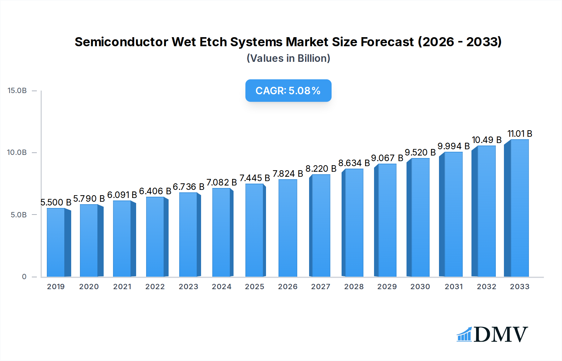
Semiconductor Wet Etch Systems Market Market Size (In Billion)
Despite the promising growth trajectory, the market faces certain restraints. The primary challenges include the stringent environmental regulations associated with wet etching chemicals and processes, requiring significant investment in waste management and compliance. Additionally, the high capital expenditure associated with acquiring state-of-the-art wet etch systems can be a barrier for smaller manufacturers. Competition from dry etching technologies, which offer certain advantages in specific applications, also presents a challenge. However, the inherent cost-effectiveness and scalability of wet etching for a wide range of applications continue to ensure its relevance. The market is segmented into Isotropic Wet Etching and Anisotropic Wet Etching, catering to diverse application needs within Logic and Memory, Power Device, MEMS, and Other Applications. Major players such as LAM Research, ACM Research, and Hitachi High Technologies America are at the forefront, driving innovation and market development across key regions including North America, Europe, and Asia.

Semiconductor Wet Etch Systems Market Company Market Share
Semiconductor Wet Etch Systems Market: Comprehensive Market Analysis and Future Outlook (2019–2033)
Report Description:
Dive into the dynamic Semiconductor Wet Etch Systems Market with this in-depth analysis, covering the period from 2019 to 2033, with a base and estimated year of 2025. This report provides unparalleled insights into market composition, trends, industry evolution, leading segments, product innovations, growth drivers, obstacles, future opportunities, and a detailed forecast. We examine the critical role of wet etching solutions in semiconductor manufacturing, from logic and memory fabrication to power devices and MEMS. Understand the strategic moves of key players, the impact of technological advancements like anisotropic wet etching, and the market's response to evolving end-user demands. This report is an essential resource for stakeholders seeking to navigate the complex landscape of semiconductor processing equipment, wafer fabrication technology, and advanced packaging solutions.
Semiconductor Wet Etch Systems Market Market Composition & Trends
The Semiconductor Wet Etch Systems Market exhibits a moderate level of concentration, with a few dominant players holding significant market share. Innovation remains a primary catalyst, driven by the relentless pursuit of smaller feature sizes, enhanced performance, and increased manufacturing efficiency in semiconductor devices. The regulatory landscape, while not directly dictating etch system technology, indirectly influences adoption through environmental compliance and safety standards for chemical usage. Substitute products, primarily dry etching technologies, present a competitive challenge, though wet etching retains its cost-effectiveness and selectivity advantages for specific applications. End-user profiles span major semiconductor manufacturers focused on logic and memory, emerging players in the power device sector, and specialized producers of MEMS and other advanced components. Mergers and acquisitions (M&A) are strategic tools for market consolidation and technology integration. M&A deal values in recent years have ranged from tens to hundreds of millions of dollars, reflecting the high stakes in this specialized market. Key trends include a growing demand for high-throughput, high-precision etching systems capable of handling complex wafer geometries and advanced materials. The shift towards panel-level packaging is also influencing system design and market opportunities.
- Market Share Distribution: Dominated by key innovators with specific technological niches.
- Innovation Catalysts: Miniaturization, performance enhancement, cost reduction, and advanced packaging demands.
- Regulatory Influence: Environmental and safety compliance for chemical usage.
- Substitute Products: Dry etching technologies, though wet etching maintains advantages in cost and selectivity.
- End-User Segments: Logic & Memory, Power Devices, MEMS, and Other Applications.
- M&A Activities: Strategic consolidation to gain technological edge and market access.
- Recent M&A Deal Values: XXX Million to XXX Million.
Semiconductor Wet Etch Systems Market Industry Evolution
The Semiconductor Wet Etch Systems Market has undergone a significant evolution, mirroring the broader advancements in the semiconductor industry. From its origins focused on simpler wafer cleaning and etching processes, the market has matured into a highly sophisticated domain driven by the ever-increasing demands for miniaturization, performance, and cost-efficiency in chip manufacturing. Over the historical period (2019–2024), the market witnessed a steady growth trajectory, fueled by the insatiable global demand for electronic devices across consumer, automotive, and industrial sectors. Technological advancements have been central to this evolution. Early wet etch systems were primarily designed for isotropic etching, offering a broad but less precise removal of material. However, the industry's shift towards intricate circuit designs and stacked architectures necessitated the development of highly selective and directional etching techniques. This led to a surge in the adoption of anisotropic wet etching capabilities, allowing for the creation of finer features with superior control. The logic and memory segment has historically been the largest driver of market growth, as these chips require the most advanced and high-volume manufacturing processes. However, the burgeoning power device market, driven by the electrification of transportation and renewable energy, has emerged as a significant growth area, demanding specialized wet etch solutions for high-power components. Similarly, the growth in the MEMS sector, enabling a new generation of sensors and actuators, has contributed to market expansion. Consumer demand for more powerful, energy-efficient, and feature-rich devices continuously pushes the boundaries of semiconductor technology, thereby propelling the need for more advanced and efficient wet etch systems. The adoption metrics for advanced wet etch systems have shown a positive trend, with manufacturers investing heavily in upgrading their facilities to incorporate these cutting-edge tools. The market has seen an average annual growth rate of approximately XX% during the historical period, with projections indicating sustained growth into the forecast period (2025–2033). This sustained growth is underpinned by ongoing research and development efforts, a strong global demand for semiconductors, and the continuous innovation in wet etching chemistries and hardware. The industry's evolution is a testament to its adaptability and its crucial role in enabling the future of electronics.
Leading Regions, Countries, or Segments in Semiconductor Wet Etch Systems Market
The Semiconductor Wet Etch Systems Market is characterized by distinct regional strengths and segment dominance. The Logic and Memory application segment consistently leads the market, driven by the enormous global demand for processors, memory chips, and other foundational components powering modern electronics. The relentless pursuit of Moore's Law, pushing for smaller and more powerful integrated circuits, necessitates highly precise and efficient wet etching processes for both front-end and back-end fabrication steps within this segment. Countries with established and expanding semiconductor manufacturing bases, such as South Korea, Taiwan, Japan, and the United States, are paramount in this dominance.
- Dominant Segment: Logic and Memory applications, accounting for an estimated XX% of the market share.
- Key Drivers:
- Massive global demand for advanced computing and data storage solutions.
- Continuous innovation in chip architecture and miniaturization.
- High-volume manufacturing requirements necessitating scalable and cost-effective etch solutions.
- Significant investments in R&D by leading foundries and integrated device manufacturers (IDMs).
- Key Drivers:
Within the Type of wet etching, Anisotropic Wet Etching is increasingly gaining prominence. While Isotropic Wet Etching remains crucial for bulk material removal and cleaning, the trend towards finer feature sizes and complex 3D structures in advanced logic and memory devices, as well as MEMS, has amplified the importance of anisotropic techniques. These methods allow for directional material removal, creating vertical sidewalls and precise etch profiles that are critical for achieving desired device functionality and performance. The increasing complexity of wafer designs demands etch processes that can precisely control the etch rate and directionality, making anisotropic wet etching indispensable for advanced semiconductor manufacturing.
- Dominant Type: Anisotropic Wet Etching, driven by the need for precise feature definition.
- Key Drivers:
- Requirement for high-aspect-ratio structures and vertical sidewalls in advanced ICs.
- Enabling complex 3D architectures in logic, memory, and MEMS devices.
- Improved process control and selectivity compared to isotropic etching.
- Development of new chemistries and etch technologies specifically for anisotropic applications.
- Key Drivers:
Geographically, Asia-Pacific, particularly Taiwan and South Korea, stands out as the dominant region. This dominance is attributable to the presence of the world's largest foundries and memory manufacturers, substantial government support for the semiconductor industry, and a robust ecosystem of material suppliers and equipment manufacturers. The region consistently leads in wafer fabrication capacity and technological adoption.
- Leading Region: Asia-Pacific, primarily Taiwan and South Korea.
- Key Drivers:
- Concentration of major semiconductor foundries and memory manufacturers.
- Significant government incentives and supportive industrial policies.
- Extensive supply chain infrastructure and R&D investments.
- High adoption rates for cutting-edge semiconductor manufacturing technologies.
- Key Drivers:
The Power Device segment is also experiencing robust growth, fueled by the global transition to electric vehicles and renewable energy sources, which require high-performance, efficient power management solutions. This segment's growth is driving demand for specialized wet etch systems capable of handling larger wafer sizes and specific material properties.
Semiconductor Wet Etch Systems Market Product Innovations
Recent product innovations in the Semiconductor Wet Etch Systems Market are revolutionizing wafer processing. Companies are focusing on developing systems that offer enhanced precision, higher throughput, and greater flexibility. For instance, systems are being designed with advanced chemistries and automation for improved anisotropic wet etching, enabling finer feature definition and better control over etch profiles essential for advanced logic and memory chips. Innovations also extend to integrated cleaning and etching functionalities, reducing processing steps and improving overall efficiency. The development of multi-chamber systems capable of handling different etch chemistries and wafer types within a single unit is a significant advancement, catering to the diverse needs of power device and MEMS manufacturing. Furthermore, the focus on sustainability is driving the development of systems with reduced chemical consumption and enhanced waste management capabilities.
Propelling Factors for Semiconductor Wet Etch Systems Market Growth
Several key factors are propelling the growth of the Semiconductor Wet Etch Systems Market. The insatiable global demand for advanced electronic devices, particularly in areas like artificial intelligence, 5G, IoT, and electric vehicles, directly translates to increased demand for semiconductor chips, thereby driving the need for sophisticated wet etch solutions. Technological advancements in chip design, such as 3D stacking and smaller feature nodes, necessitate more precise and efficient etching processes. Government initiatives supporting domestic semiconductor manufacturing, coupled with growing investments in research and development by semiconductor giants, are creating a favorable market environment. The cost-effectiveness and high selectivity of wet etching for specific applications, especially in cleaning and certain material removal processes, continue to make it an indispensable part of the semiconductor fabrication workflow.
- Key Growth Drivers:
- Surging demand for advanced electronic devices and semiconductors.
- Technological advancements in chip design (e.g., 3D stacking, smaller nodes).
- Supportive government policies and R&D investments.
- Cost-effectiveness and high selectivity of wet etching for specific applications.
Obstacles in the Semiconductor Wet Etch Systems Market Market
Despite robust growth, the Semiconductor Wet Etch Systems Market faces several obstacles. Stringent environmental regulations regarding the use and disposal of hazardous chemicals employed in wet etching processes pose a significant challenge, increasing operational costs and compliance burdens. Geopolitical tensions and trade disputes can disrupt global supply chains for critical raw materials and components, leading to production delays and increased costs. The intense competition from dry etching technologies, which offer certain advantages in specific applications, continues to exert pressure. Furthermore, the high capital expenditure required for advanced wet etch systems can be a barrier for smaller manufacturers or those in emerging markets. Ensuring consistent quality and yield in large-scale manufacturing remains a perpetual challenge, requiring continuous process optimization.
- Key Obstacles:
- Stringent environmental regulations on chemical usage and disposal.
- Global supply chain disruptions and geopolitical uncertainties.
- Competition from dry etching technologies.
- High capital investment for advanced systems.
- Maintaining process consistency and yield in high-volume manufacturing.
Future Opportunities in Semiconductor Wet Etch Systems Market
The Semiconductor Wet Etch Systems Market is poised for significant future opportunities. The burgeoning market for advanced packaging solutions, such as fan-out wafer-level packaging (FOWLP) and chiplets, presents a substantial growth avenue, requiring specialized wet etch capabilities for precise wafer preparation and interconnect formation. The continued expansion of the power device market, driven by electrification and renewable energy, will fuel demand for specialized etching systems. Innovations in new materials for semiconductors, such as wide-bandgap semiconductors, will require novel wet etch chemistries and processes. The increasing adoption of automation and AI in semiconductor manufacturing offers opportunities for developing intelligent wet etch systems that can optimize processes in real-time and enhance yield. Furthermore, emerging applications in areas like advanced sensors, quantum computing, and specialized medical devices will create new niche markets for tailored wet etch solutions.
- Emerging Opportunities:
- Growth in advanced packaging solutions (FOWLP, chiplets).
- Expanding market for power devices and electric vehicles.
- Development of etch processes for novel semiconductor materials.
- Integration of AI and automation in wet etch systems.
- Niche markets in advanced sensors and quantum computing.
Major Players in the Semiconductor Wet Etch Systems Market Ecosystem
- ACM Research
- LAM Research
- Hitachi High Technologies America
- Alfa Laval Inc
- Veeco Instruments Inc
- JST Manufacturing Inc
- Modutek Corporation
- Inseto
- Shenzhen Dragon Etching Co Ltd
- Micronit BV
Key Developments in Semiconductor Wet Etch Systems Market Industry
- September 2024: ACM Research Inc. unveiled its Ultra C bev-p panel bevel etching tool, tailored for fan-out panel-level packaging (FOPLP) applications. This innovative tool specializes in bevel etching and cleaning for copper-related processes. Notably, it can manage bevel etching on both the front and back sides of the panel, all within a single system. Such versatility boosts process efficiency and bolsters product reliability.
- August 2024: Veeco Instruments Inc. revealed that IBM had chosen its WaferStorm Wet Processing System for Advanced Packaging applications. Furthermore, the two companies have inked a joint development agreement. This collaboration aims to delve into advanced packaging applications, leveraging various wet processing technologies from Veeco. As part of this partnership, the WaferStorm Wet Processing System will find its home at the Albany NanoTech Complex in Albany, NY. This facility is a hub for IBM and its ecosystem partners, who are at the forefront of R&D in advanced packaging and chiplet technologies.
Strategic Semiconductor Wet Etch Systems Market Market Forecast
The Semiconductor Wet Etch Systems Market is projected for robust growth throughout the forecast period (2025–2033). The accelerating demand for advanced semiconductor devices across diverse sectors, coupled with continuous technological innovation in chip architecture and materials, will remain the primary growth catalysts. The increasing adoption of advanced packaging techniques and the expanding market for power devices will further drive the need for specialized wet etch solutions. Strategic investments in R&D and manufacturing capacity by key players, along with supportive government policies in major semiconductor-producing regions, will foster market expansion. Emerging opportunities in niche applications and the integration of intelligent automation will present new avenues for growth, ensuring the market's dynamic evolution and sustained profitability. The overall market is expected to witness a compound annual growth rate (CAGR) of approximately XX% during the forecast period, reaching an estimated XXXX Million by 2033.
Semiconductor Wet Etch Systems Market Segmentation
-
1. Type
- 1.1. Isotropic Wet Etching
- 1.2. Anisotropic Wet Etching
-
2. Application
- 2.1. Logic and Memory
- 2.2. Power Device
- 2.3. MEMS
- 2.4. Other Applications
Semiconductor Wet Etch Systems Market Segmentation By Geography
- 1. North America
- 2. Europe
- 3. Asia
- 4. Australia and New Zealand
- 5. Latin America
- 6. Middle East and Africa
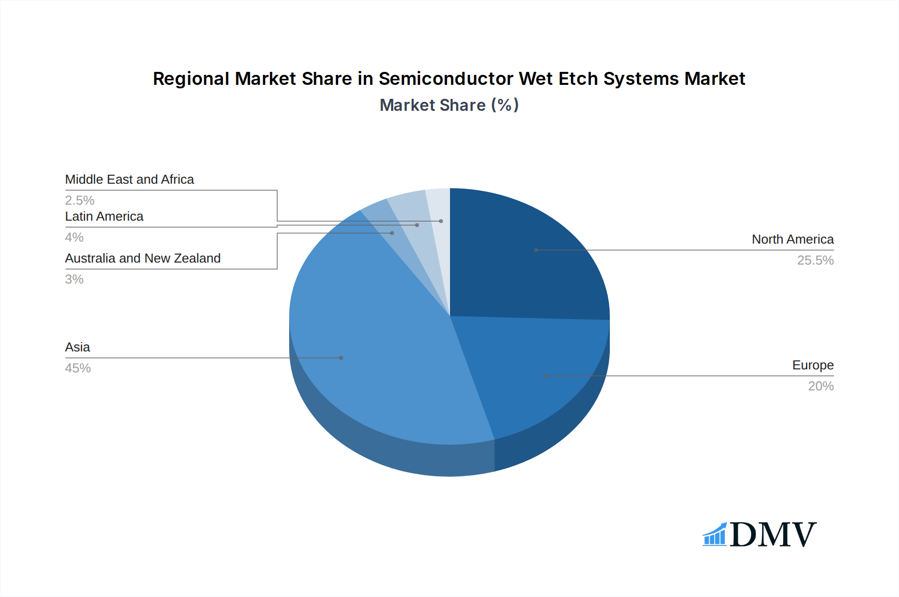
Semiconductor Wet Etch Systems Market Regional Market Share
Geographic Coverage of Semiconductor Wet Etch Systems Market
Semiconductor Wet Etch Systems Market REPORT HIGHLIGHTS
| Aspects | Details |
|---|---|
| Study Period | 2020-2034 |
| Base Year | 2025 |
| Estimated Year | 2026 |
| Forecast Period | 2026-2034 |
| Historical Period | 2020-2025 |
| Growth Rate | CAGR of 5.35% from 2020-2034 |
| Segmentation |
|
Table of Contents
- 1. Introduction
- 1.1. Research Scope
- 1.2. Market Segmentation
- 1.3. Research Objective
- 1.4. Definitions and Assumptions
- 2. Executive Summary
- 2.1. Market Snapshot
- 3. Market Dynamics
- 3.1. Market Drivers
- 3.2. Market Restrains
- 3.3. Market Trends
- 3.4. Market Opportunities
- 4. Market Factor Analysis
- 4.1. Porters Five Forces
- 4.1.1. Bargaining Power of Suppliers
- 4.1.2. Bargaining Power of Buyers
- 4.1.3. Threat of New Entrants
- 4.1.4. Threat of Substitutes
- 4.1.5. Competitive Rivalry
- 4.2. PESTEL analysis
- 4.3. BCG Analysis
- 4.3.1. Stars (High Growth, High Market Share)
- 4.3.2. Cash Cows (Low Growth, High Market Share)
- 4.3.3. Question Mark (High Growth, Low Market Share)
- 4.3.4. Dogs (Low Growth, Low Market Share)
- 4.4. Ansoff Matrix Analysis
- 4.5. Supply Chain Analysis
- 4.6. Regulatory Landscape
- 4.7. Current Market Potential and Opportunity Assessment (TAM–SAM–SOM Framework)
- 4.8. DMV Analyst Note
- 4.1. Porters Five Forces
- 5. Market Analysis, Insights and Forecast 2021-2033
- 5.1. Market Analysis, Insights and Forecast - by Type
- 5.1.1. Isotropic Wet Etching
- 5.1.2. Anisotropic Wet Etching
- 5.2. Market Analysis, Insights and Forecast - by Application
- 5.2.1. Logic and Memory
- 5.2.2. Power Device
- 5.2.3. MEMS
- 5.2.4. Other Applications
- 5.3. Market Analysis, Insights and Forecast - by Region
- 5.3.1. North America
- 5.3.2. Europe
- 5.3.3. Asia
- 5.3.4. Australia and New Zealand
- 5.3.5. Latin America
- 5.3.6. Middle East and Africa
- 5.1. Market Analysis, Insights and Forecast - by Type
- 6. Global Semiconductor Wet Etch Systems Market Analysis, Insights and Forecast, 2021-2033
- 6.1. Market Analysis, Insights and Forecast - by Type
- 6.1.1. Isotropic Wet Etching
- 6.1.2. Anisotropic Wet Etching
- 6.2. Market Analysis, Insights and Forecast - by Application
- 6.2.1. Logic and Memory
- 6.2.2. Power Device
- 6.2.3. MEMS
- 6.2.4. Other Applications
- 6.1. Market Analysis, Insights and Forecast - by Type
- 7. North America Semiconductor Wet Etch Systems Market Analysis, Insights and Forecast, 2020-2032
- 7.1. Market Analysis, Insights and Forecast - by Type
- 7.1.1. Isotropic Wet Etching
- 7.1.2. Anisotropic Wet Etching
- 7.2. Market Analysis, Insights and Forecast - by Application
- 7.2.1. Logic and Memory
- 7.2.2. Power Device
- 7.2.3. MEMS
- 7.2.4. Other Applications
- 7.1. Market Analysis, Insights and Forecast - by Type
- 8. Europe Semiconductor Wet Etch Systems Market Analysis, Insights and Forecast, 2020-2032
- 8.1. Market Analysis, Insights and Forecast - by Type
- 8.1.1. Isotropic Wet Etching
- 8.1.2. Anisotropic Wet Etching
- 8.2. Market Analysis, Insights and Forecast - by Application
- 8.2.1. Logic and Memory
- 8.2.2. Power Device
- 8.2.3. MEMS
- 8.2.4. Other Applications
- 8.1. Market Analysis, Insights and Forecast - by Type
- 9. Asia Semiconductor Wet Etch Systems Market Analysis, Insights and Forecast, 2020-2032
- 9.1. Market Analysis, Insights and Forecast - by Type
- 9.1.1. Isotropic Wet Etching
- 9.1.2. Anisotropic Wet Etching
- 9.2. Market Analysis, Insights and Forecast - by Application
- 9.2.1. Logic and Memory
- 9.2.2. Power Device
- 9.2.3. MEMS
- 9.2.4. Other Applications
- 9.1. Market Analysis, Insights and Forecast - by Type
- 10. Australia and New Zealand Semiconductor Wet Etch Systems Market Analysis, Insights and Forecast, 2020-2032
- 10.1. Market Analysis, Insights and Forecast - by Type
- 10.1.1. Isotropic Wet Etching
- 10.1.2. Anisotropic Wet Etching
- 10.2. Market Analysis, Insights and Forecast - by Application
- 10.2.1. Logic and Memory
- 10.2.2. Power Device
- 10.2.3. MEMS
- 10.2.4. Other Applications
- 10.1. Market Analysis, Insights and Forecast - by Type
- 11. Latin America Semiconductor Wet Etch Systems Market Analysis, Insights and Forecast, 2020-2032
- 11.1. Market Analysis, Insights and Forecast - by Type
- 11.1.1. Isotropic Wet Etching
- 11.1.2. Anisotropic Wet Etching
- 11.2. Market Analysis, Insights and Forecast - by Application
- 11.2.1. Logic and Memory
- 11.2.2. Power Device
- 11.2.3. MEMS
- 11.2.4. Other Applications
- 11.1. Market Analysis, Insights and Forecast - by Type
- 12. Middle East and Africa Semiconductor Wet Etch Systems Market Analysis, Insights and Forecast, 2020-2032
- 12.1. Market Analysis, Insights and Forecast - by Type
- 12.1.1. Isotropic Wet Etching
- 12.1.2. Anisotropic Wet Etching
- 12.2. Market Analysis, Insights and Forecast - by Application
- 12.2.1. Logic and Memory
- 12.2.2. Power Device
- 12.2.3. MEMS
- 12.2.4. Other Applications
- 12.1. Market Analysis, Insights and Forecast - by Type
- 13. Competitive Analysis
- 13.1. Company Profiles
- 13.1.1 ACM Research
- 13.1.1.1. Company Overview
- 13.1.1.2. Products
- 13.1.1.3. Company Financials
- 13.1.1.4. SWOT Analysis
- 13.1.2 LAM Research
- 13.1.2.1. Company Overview
- 13.1.2.2. Products
- 13.1.2.3. Company Financials
- 13.1.2.4. SWOT Analysis
- 13.1.3 Hitachi High Technologies America
- 13.1.3.1. Company Overview
- 13.1.3.2. Products
- 13.1.3.3. Company Financials
- 13.1.3.4. SWOT Analysis
- 13.1.4 Alfa Laval Inc
- 13.1.4.1. Company Overview
- 13.1.4.2. Products
- 13.1.4.3. Company Financials
- 13.1.4.4. SWOT Analysis
- 13.1.5 Veeco Instruments Inc
- 13.1.5.1. Company Overview
- 13.1.5.2. Products
- 13.1.5.3. Company Financials
- 13.1.5.4. SWOT Analysis
- 13.1.6 JST Manufacturing Inc
- 13.1.6.1. Company Overview
- 13.1.6.2. Products
- 13.1.6.3. Company Financials
- 13.1.6.4. SWOT Analysis
- 13.1.7 Modutek Corporation
- 13.1.7.1. Company Overview
- 13.1.7.2. Products
- 13.1.7.3. Company Financials
- 13.1.7.4. SWOT Analysis
- 13.1.8 Inseto
- 13.1.8.1. Company Overview
- 13.1.8.2. Products
- 13.1.8.3. Company Financials
- 13.1.8.4. SWOT Analysis
- 13.1.9 Shenzhen Dragon Etching Co Ltd
- 13.1.9.1. Company Overview
- 13.1.9.2. Products
- 13.1.9.3. Company Financials
- 13.1.9.4. SWOT Analysis
- 13.1.10 Micronit BV*List Not Exhaustive
- 13.1.10.1. Company Overview
- 13.1.10.2. Products
- 13.1.10.3. Company Financials
- 13.1.10.4. SWOT Analysis
- 13.1.1 ACM Research
- 13.2. Market Entropy
- 13.2.1 Company's Key Areas Served
- 13.2.2 Recent Developments
- 13.3. Company Market Share Analysis 2025
- 13.3.1 Top 5 Companies Market Share Analysis
- 13.3.2 Top 3 Companies Market Share Analysis
- 13.4. List of Potential Customers
- 14. Research Methodology
List of Figures
- Figure 1: Global Semiconductor Wet Etch Systems Market Revenue Breakdown (Million, %) by Region 2025 & 2033
- Figure 2: Global Semiconductor Wet Etch Systems Market Volume Breakdown (Billion, %) by Region 2025 & 2033
- Figure 3: North America Semiconductor Wet Etch Systems Market Revenue (Million), by Type 2025 & 2033
- Figure 4: North America Semiconductor Wet Etch Systems Market Volume (Billion), by Type 2025 & 2033
- Figure 5: North America Semiconductor Wet Etch Systems Market Revenue Share (%), by Type 2025 & 2033
- Figure 6: North America Semiconductor Wet Etch Systems Market Volume Share (%), by Type 2025 & 2033
- Figure 7: North America Semiconductor Wet Etch Systems Market Revenue (Million), by Application 2025 & 2033
- Figure 8: North America Semiconductor Wet Etch Systems Market Volume (Billion), by Application 2025 & 2033
- Figure 9: North America Semiconductor Wet Etch Systems Market Revenue Share (%), by Application 2025 & 2033
- Figure 10: North America Semiconductor Wet Etch Systems Market Volume Share (%), by Application 2025 & 2033
- Figure 11: North America Semiconductor Wet Etch Systems Market Revenue (Million), by Country 2025 & 2033
- Figure 12: North America Semiconductor Wet Etch Systems Market Volume (Billion), by Country 2025 & 2033
- Figure 13: North America Semiconductor Wet Etch Systems Market Revenue Share (%), by Country 2025 & 2033
- Figure 14: North America Semiconductor Wet Etch Systems Market Volume Share (%), by Country 2025 & 2033
- Figure 15: Europe Semiconductor Wet Etch Systems Market Revenue (Million), by Type 2025 & 2033
- Figure 16: Europe Semiconductor Wet Etch Systems Market Volume (Billion), by Type 2025 & 2033
- Figure 17: Europe Semiconductor Wet Etch Systems Market Revenue Share (%), by Type 2025 & 2033
- Figure 18: Europe Semiconductor Wet Etch Systems Market Volume Share (%), by Type 2025 & 2033
- Figure 19: Europe Semiconductor Wet Etch Systems Market Revenue (Million), by Application 2025 & 2033
- Figure 20: Europe Semiconductor Wet Etch Systems Market Volume (Billion), by Application 2025 & 2033
- Figure 21: Europe Semiconductor Wet Etch Systems Market Revenue Share (%), by Application 2025 & 2033
- Figure 22: Europe Semiconductor Wet Etch Systems Market Volume Share (%), by Application 2025 & 2033
- Figure 23: Europe Semiconductor Wet Etch Systems Market Revenue (Million), by Country 2025 & 2033
- Figure 24: Europe Semiconductor Wet Etch Systems Market Volume (Billion), by Country 2025 & 2033
- Figure 25: Europe Semiconductor Wet Etch Systems Market Revenue Share (%), by Country 2025 & 2033
- Figure 26: Europe Semiconductor Wet Etch Systems Market Volume Share (%), by Country 2025 & 2033
- Figure 27: Asia Semiconductor Wet Etch Systems Market Revenue (Million), by Type 2025 & 2033
- Figure 28: Asia Semiconductor Wet Etch Systems Market Volume (Billion), by Type 2025 & 2033
- Figure 29: Asia Semiconductor Wet Etch Systems Market Revenue Share (%), by Type 2025 & 2033
- Figure 30: Asia Semiconductor Wet Etch Systems Market Volume Share (%), by Type 2025 & 2033
- Figure 31: Asia Semiconductor Wet Etch Systems Market Revenue (Million), by Application 2025 & 2033
- Figure 32: Asia Semiconductor Wet Etch Systems Market Volume (Billion), by Application 2025 & 2033
- Figure 33: Asia Semiconductor Wet Etch Systems Market Revenue Share (%), by Application 2025 & 2033
- Figure 34: Asia Semiconductor Wet Etch Systems Market Volume Share (%), by Application 2025 & 2033
- Figure 35: Asia Semiconductor Wet Etch Systems Market Revenue (Million), by Country 2025 & 2033
- Figure 36: Asia Semiconductor Wet Etch Systems Market Volume (Billion), by Country 2025 & 2033
- Figure 37: Asia Semiconductor Wet Etch Systems Market Revenue Share (%), by Country 2025 & 2033
- Figure 38: Asia Semiconductor Wet Etch Systems Market Volume Share (%), by Country 2025 & 2033
- Figure 39: Australia and New Zealand Semiconductor Wet Etch Systems Market Revenue (Million), by Type 2025 & 2033
- Figure 40: Australia and New Zealand Semiconductor Wet Etch Systems Market Volume (Billion), by Type 2025 & 2033
- Figure 41: Australia and New Zealand Semiconductor Wet Etch Systems Market Revenue Share (%), by Type 2025 & 2033
- Figure 42: Australia and New Zealand Semiconductor Wet Etch Systems Market Volume Share (%), by Type 2025 & 2033
- Figure 43: Australia and New Zealand Semiconductor Wet Etch Systems Market Revenue (Million), by Application 2025 & 2033
- Figure 44: Australia and New Zealand Semiconductor Wet Etch Systems Market Volume (Billion), by Application 2025 & 2033
- Figure 45: Australia and New Zealand Semiconductor Wet Etch Systems Market Revenue Share (%), by Application 2025 & 2033
- Figure 46: Australia and New Zealand Semiconductor Wet Etch Systems Market Volume Share (%), by Application 2025 & 2033
- Figure 47: Australia and New Zealand Semiconductor Wet Etch Systems Market Revenue (Million), by Country 2025 & 2033
- Figure 48: Australia and New Zealand Semiconductor Wet Etch Systems Market Volume (Billion), by Country 2025 & 2033
- Figure 49: Australia and New Zealand Semiconductor Wet Etch Systems Market Revenue Share (%), by Country 2025 & 2033
- Figure 50: Australia and New Zealand Semiconductor Wet Etch Systems Market Volume Share (%), by Country 2025 & 2033
- Figure 51: Latin America Semiconductor Wet Etch Systems Market Revenue (Million), by Type 2025 & 2033
- Figure 52: Latin America Semiconductor Wet Etch Systems Market Volume (Billion), by Type 2025 & 2033
- Figure 53: Latin America Semiconductor Wet Etch Systems Market Revenue Share (%), by Type 2025 & 2033
- Figure 54: Latin America Semiconductor Wet Etch Systems Market Volume Share (%), by Type 2025 & 2033
- Figure 55: Latin America Semiconductor Wet Etch Systems Market Revenue (Million), by Application 2025 & 2033
- Figure 56: Latin America Semiconductor Wet Etch Systems Market Volume (Billion), by Application 2025 & 2033
- Figure 57: Latin America Semiconductor Wet Etch Systems Market Revenue Share (%), by Application 2025 & 2033
- Figure 58: Latin America Semiconductor Wet Etch Systems Market Volume Share (%), by Application 2025 & 2033
- Figure 59: Latin America Semiconductor Wet Etch Systems Market Revenue (Million), by Country 2025 & 2033
- Figure 60: Latin America Semiconductor Wet Etch Systems Market Volume (Billion), by Country 2025 & 2033
- Figure 61: Latin America Semiconductor Wet Etch Systems Market Revenue Share (%), by Country 2025 & 2033
- Figure 62: Latin America Semiconductor Wet Etch Systems Market Volume Share (%), by Country 2025 & 2033
- Figure 63: Middle East and Africa Semiconductor Wet Etch Systems Market Revenue (Million), by Type 2025 & 2033
- Figure 64: Middle East and Africa Semiconductor Wet Etch Systems Market Volume (Billion), by Type 2025 & 2033
- Figure 65: Middle East and Africa Semiconductor Wet Etch Systems Market Revenue Share (%), by Type 2025 & 2033
- Figure 66: Middle East and Africa Semiconductor Wet Etch Systems Market Volume Share (%), by Type 2025 & 2033
- Figure 67: Middle East and Africa Semiconductor Wet Etch Systems Market Revenue (Million), by Application 2025 & 2033
- Figure 68: Middle East and Africa Semiconductor Wet Etch Systems Market Volume (Billion), by Application 2025 & 2033
- Figure 69: Middle East and Africa Semiconductor Wet Etch Systems Market Revenue Share (%), by Application 2025 & 2033
- Figure 70: Middle East and Africa Semiconductor Wet Etch Systems Market Volume Share (%), by Application 2025 & 2033
- Figure 71: Middle East and Africa Semiconductor Wet Etch Systems Market Revenue (Million), by Country 2025 & 2033
- Figure 72: Middle East and Africa Semiconductor Wet Etch Systems Market Volume (Billion), by Country 2025 & 2033
- Figure 73: Middle East and Africa Semiconductor Wet Etch Systems Market Revenue Share (%), by Country 2025 & 2033
- Figure 74: Middle East and Africa Semiconductor Wet Etch Systems Market Volume Share (%), by Country 2025 & 2033
List of Tables
- Table 1: Global Semiconductor Wet Etch Systems Market Revenue Million Forecast, by Type 2020 & 2033
- Table 2: Global Semiconductor Wet Etch Systems Market Volume Billion Forecast, by Type 2020 & 2033
- Table 3: Global Semiconductor Wet Etch Systems Market Revenue Million Forecast, by Application 2020 & 2033
- Table 4: Global Semiconductor Wet Etch Systems Market Volume Billion Forecast, by Application 2020 & 2033
- Table 5: Global Semiconductor Wet Etch Systems Market Revenue Million Forecast, by Region 2020 & 2033
- Table 6: Global Semiconductor Wet Etch Systems Market Volume Billion Forecast, by Region 2020 & 2033
- Table 7: Global Semiconductor Wet Etch Systems Market Revenue Million Forecast, by Type 2020 & 2033
- Table 8: Global Semiconductor Wet Etch Systems Market Volume Billion Forecast, by Type 2020 & 2033
- Table 9: Global Semiconductor Wet Etch Systems Market Revenue Million Forecast, by Application 2020 & 2033
- Table 10: Global Semiconductor Wet Etch Systems Market Volume Billion Forecast, by Application 2020 & 2033
- Table 11: Global Semiconductor Wet Etch Systems Market Revenue Million Forecast, by Country 2020 & 2033
- Table 12: Global Semiconductor Wet Etch Systems Market Volume Billion Forecast, by Country 2020 & 2033
- Table 13: Global Semiconductor Wet Etch Systems Market Revenue Million Forecast, by Type 2020 & 2033
- Table 14: Global Semiconductor Wet Etch Systems Market Volume Billion Forecast, by Type 2020 & 2033
- Table 15: Global Semiconductor Wet Etch Systems Market Revenue Million Forecast, by Application 2020 & 2033
- Table 16: Global Semiconductor Wet Etch Systems Market Volume Billion Forecast, by Application 2020 & 2033
- Table 17: Global Semiconductor Wet Etch Systems Market Revenue Million Forecast, by Country 2020 & 2033
- Table 18: Global Semiconductor Wet Etch Systems Market Volume Billion Forecast, by Country 2020 & 2033
- Table 19: Global Semiconductor Wet Etch Systems Market Revenue Million Forecast, by Type 2020 & 2033
- Table 20: Global Semiconductor Wet Etch Systems Market Volume Billion Forecast, by Type 2020 & 2033
- Table 21: Global Semiconductor Wet Etch Systems Market Revenue Million Forecast, by Application 2020 & 2033
- Table 22: Global Semiconductor Wet Etch Systems Market Volume Billion Forecast, by Application 2020 & 2033
- Table 23: Global Semiconductor Wet Etch Systems Market Revenue Million Forecast, by Country 2020 & 2033
- Table 24: Global Semiconductor Wet Etch Systems Market Volume Billion Forecast, by Country 2020 & 2033
- Table 25: Global Semiconductor Wet Etch Systems Market Revenue Million Forecast, by Type 2020 & 2033
- Table 26: Global Semiconductor Wet Etch Systems Market Volume Billion Forecast, by Type 2020 & 2033
- Table 27: Global Semiconductor Wet Etch Systems Market Revenue Million Forecast, by Application 2020 & 2033
- Table 28: Global Semiconductor Wet Etch Systems Market Volume Billion Forecast, by Application 2020 & 2033
- Table 29: Global Semiconductor Wet Etch Systems Market Revenue Million Forecast, by Country 2020 & 2033
- Table 30: Global Semiconductor Wet Etch Systems Market Volume Billion Forecast, by Country 2020 & 2033
- Table 31: Global Semiconductor Wet Etch Systems Market Revenue Million Forecast, by Type 2020 & 2033
- Table 32: Global Semiconductor Wet Etch Systems Market Volume Billion Forecast, by Type 2020 & 2033
- Table 33: Global Semiconductor Wet Etch Systems Market Revenue Million Forecast, by Application 2020 & 2033
- Table 34: Global Semiconductor Wet Etch Systems Market Volume Billion Forecast, by Application 2020 & 2033
- Table 35: Global Semiconductor Wet Etch Systems Market Revenue Million Forecast, by Country 2020 & 2033
- Table 36: Global Semiconductor Wet Etch Systems Market Volume Billion Forecast, by Country 2020 & 2033
- Table 37: Global Semiconductor Wet Etch Systems Market Revenue Million Forecast, by Type 2020 & 2033
- Table 38: Global Semiconductor Wet Etch Systems Market Volume Billion Forecast, by Type 2020 & 2033
- Table 39: Global Semiconductor Wet Etch Systems Market Revenue Million Forecast, by Application 2020 & 2033
- Table 40: Global Semiconductor Wet Etch Systems Market Volume Billion Forecast, by Application 2020 & 2033
- Table 41: Global Semiconductor Wet Etch Systems Market Revenue Million Forecast, by Country 2020 & 2033
- Table 42: Global Semiconductor Wet Etch Systems Market Volume Billion Forecast, by Country 2020 & 2033
Frequently Asked Questions
1. What is the projected Compound Annual Growth Rate (CAGR) of the Semiconductor Wet Etch Systems Market?
The projected CAGR is approximately 5.35%.
2. Which companies are prominent players in the Semiconductor Wet Etch Systems Market?
Key companies in the market include ACM Research, LAM Research, Hitachi High Technologies America, Alfa Laval Inc, Veeco Instruments Inc, JST Manufacturing Inc, Modutek Corporation, Inseto, Shenzhen Dragon Etching Co Ltd, Micronit BV*List Not Exhaustive.
3. What are the main segments of the Semiconductor Wet Etch Systems Market?
The market segments include Type, Application.
4. Can you provide details about the market size?
The market size is estimated to be USD 5.5 Million as of 2022.
5. What are some drivers contributing to market growth?
Increasing Application in Consumer Electronic Devices. Automotive. and Aerospace; Proliferation of Artificial Intelligence. IoT. and Connected Devices across Industry Verticals.
6. What are the notable trends driving market growth?
The MEMS Segment is Expected to Observe Significant Growth.
7. Are there any restraints impacting market growth?
Increasing Application in Consumer Electronic Devices. Automotive. and Aerospace; Proliferation of Artificial Intelligence. IoT. and Connected Devices across Industry Verticals.
8. Can you provide examples of recent developments in the market?
September 2024: ACM Research Inc. unveiled its Ultra C bev-p panel bevel etching tool, tailored for fan-out panel-level packaging (FOPLP) applications. This innovative tool specializes in bevel etching and cleaning for copper-related processes. Notably, it can manage bevel etching on both the front and back sides of the panel, all within a single system. Such versatility boosts process efficiency and bolsters product reliability.August 2024: Veeco Instruments Inc. revealed that IBM had chosen its WaferStorm Wet Processing System for Advanced Packaging applications. Furthermore, the two companies have inked a joint development agreement. This collaboration aims to delve into advanced packaging applications, leveraging various wet processing technologies from Veeco. As part of this partnership, the WaferStorm Wet Processing System will find its home at the Albany NanoTech Complex in Albany, NY. This facility is a hub for IBM and its ecosystem partners, who are at the forefront of R&D in advanced packaging and chiplet technologies.
9. What pricing options are available for accessing the report?
Pricing options include single-user, multi-user, and enterprise licenses priced at USD 4750, USD 5250, and USD 8750 respectively.
10. Is the market size provided in terms of value or volume?
The market size is provided in terms of value, measured in Million and volume, measured in Billion.
11. Are there any specific market keywords associated with the report?
Yes, the market keyword associated with the report is "Semiconductor Wet Etch Systems Market," which aids in identifying and referencing the specific market segment covered.
12. How do I determine which pricing option suits my needs best?
The pricing options vary based on user requirements and access needs. Individual users may opt for single-user licenses, while businesses requiring broader access may choose multi-user or enterprise licenses for cost-effective access to the report.
13. Are there any additional resources or data provided in the Semiconductor Wet Etch Systems Market report?
While the report offers comprehensive insights, it's advisable to review the specific contents or supplementary materials provided to ascertain if additional resources or data are available.
14. How can I stay updated on further developments or reports in the Semiconductor Wet Etch Systems Market?
To stay informed about further developments, trends, and reports in the Semiconductor Wet Etch Systems Market, consider subscribing to industry newsletters, following relevant companies and organizations, or regularly checking reputable industry news sources and publications.
Methodology
Step 1 - Identification of Relevant Samples Size from Population Database


Step 2 - Approaches for Defining Global Market Size (Value, Volume* & Price*)

Note*: In applicable scenarios
Step 3 - Data Sources
Primary Research
- Web Analytics
- Survey Reports
- Research Institute
- Latest Research Reports
- Opinion Leaders
Secondary Research
- Annual Reports
- White Paper
- Latest Press Release
- Industry Association
- Paid Database
- Investor Presentations

Step 4 - Data Triangulation
Involves using different sources of information in order to increase the validity of a study
These sources are likely to be stakeholders in a program - participants, other researchers, program staff, other community members, and so on.
Then we put all data in single framework & apply various statistical tools to find out the dynamic on the market.
During the analysis stage, feedback from the stakeholder groups would be compared to determine areas of agreement as well as areas of divergence