

Key Insights
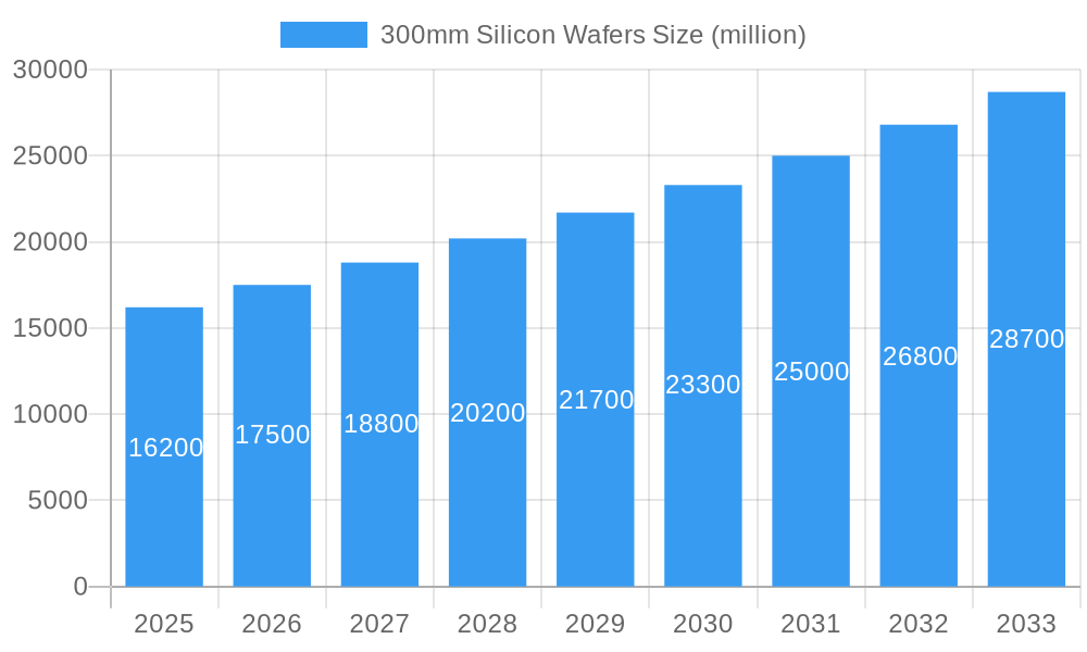
The 300mm silicon wafer market is experiencing robust growth, driven by the increasing demand for advanced semiconductor devices in various applications, including 5G infrastructure, high-performance computing (HPC), and artificial intelligence (AI). The market's expansion is fueled by continuous advancements in semiconductor technology, requiring larger and higher-quality wafers to accommodate increasingly complex chip designs. While the precise market size for 2025 is unavailable, considering a reasonable CAGR of 8% (a conservative estimate given industry trends) and a hypothetical 2024 market size of $15 billion, we can project a 2025 market value of approximately $16.2 billion. This growth is anticipated to continue throughout the forecast period (2025-2033), though at a potentially moderating rate as the market matures. Key players such as Shin-Etsu Chemical, SUMCO, and Siltronic are strategically investing in capacity expansion and technological improvements to meet this rising demand.
300mm Silicon Wafers Market Size (In Billion)
However, the market also faces certain challenges. Supply chain disruptions, geopolitical instability, and the cyclical nature of the semiconductor industry can impact growth trajectory. Furthermore, the increasing complexity and cost of manufacturing 300mm wafers present obstacles to new entrants. Nevertheless, long-term prospects remain positive, driven by the inevitable shift towards advanced semiconductor nodes and the expanding applications of sophisticated electronics across diverse industries. Technological advancements such as improving wafer quality and yield rates will further contribute to market expansion, while efforts to enhance supply chain resilience will mitigate potential risks. Regional variations in growth rates are expected, with regions like Asia-Pacific potentially exhibiting faster growth due to the concentration of semiconductor manufacturing facilities in the region.
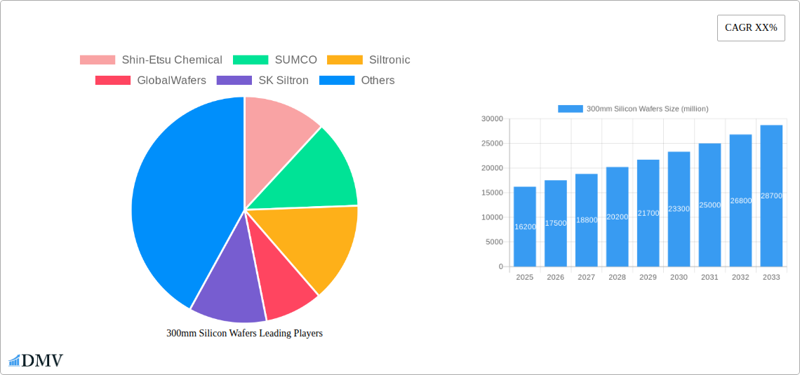
300mm Silicon Wafers Company Market Share
300mm Silicon Wafers Market Report: 2019-2033 Forecast
This comprehensive report provides a detailed analysis of the global 300mm silicon wafer market, offering invaluable insights for stakeholders across the semiconductor industry. Covering the period 2019-2033, with a base year of 2025 and a forecast period of 2025-2033, this study unravels market dynamics, technological advancements, and future growth potential. Key players such as Shin-Etsu Chemical, SUMCO, Siltronic, GlobalWafers, SK Siltron, SOITEC, Zing Semiconductor Corporation, Ferrotec, and Kinik are meticulously analyzed, providing a complete picture of this vital sector. The report quantifies market values in millions, offering precise data points for informed decision-making.
300mm Silicon Wafers Market Composition & Trends
The 300mm silicon wafer market is characterized by high concentration amongst leading players. Shin-Etsu Chemical, SUMCO, and Siltronic collectively control a significant portion – estimated at xx million USD – of the global market share in 2025. Innovation is driven by the relentless pursuit of higher yields, improved wafer quality, and cost reduction. Stringent regulatory landscapes, particularly concerning environmental impact and material sourcing, influence manufacturing practices. While substitutes exist, their limited performance characteristics maintain the dominance of 300mm silicon wafers. End-users primarily comprise major semiconductor manufacturers serving diverse applications including logic, memory, and power devices. M&A activity, though not exceedingly frequent, has witnessed significant deal values in recent years, with deals totaling an estimated xx million USD between 2019 and 2024.
- Market Share Distribution (2025): Shin-Etsu Chemical (xx%), SUMCO (xx%), Siltronic (xx%), Others (xx%).
- M&A Activity (2019-2024): Total deal value estimated at xx million USD.
- Key End-Users: Logic chip manufacturers, Memory chip manufacturers, Power device manufacturers.
300mm Silicon Wafers Industry Evolution
The 300mm silicon wafer market exhibits a robust growth trajectory, driven primarily by the increasing demand for advanced semiconductor devices. The historical period (2019-2024) saw a Compound Annual Growth Rate (CAGR) of approximately xx%, reaching a market value of xx million USD in 2024. Technological advancements, such as the development of improved crystal growth techniques and surface polishing methods, continue to push the boundaries of wafer quality and performance. Simultaneously, shifting consumer demands, particularly for faster and more energy-efficient electronics, fuel the need for higher-performance silicon wafers. We project a CAGR of xx% during the forecast period (2025-2033), reaching a projected market value of xx million USD by 2033. This growth is fueled by rising adoption in the automotive, 5G, and AI sectors.
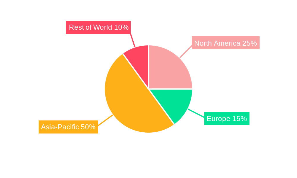
Leading Regions, Countries, or Segments in 300mm Silicon Wafers
The Asia-Pacific region, specifically Taiwan, South Korea, and Japan, holds a dominant position in the 300mm silicon wafer market, accounting for xx% of the global market share in 2025. This dominance stems from several factors:
- High Concentration of Semiconductor Manufacturers: The region boasts a significant concentration of leading semiconductor fabrication plants.
- Significant Government Investment: Governments in the region are actively investing in the semiconductor industry, providing incentives for infrastructure development and technological advancements.
- Robust Supply Chain Ecosystem: The presence of a well-established supply chain ecosystem, from raw materials to manufacturing, further bolsters the region's dominance.
This leadership position is expected to remain throughout the forecast period, although other regions like North America and Europe are expected to see modest growth.
300mm Silicon Wafers Product Innovations
Recent innovations in 300mm silicon wafers center on enhancing crystal quality, reducing defect density, and improving surface flatness. This translates to improved chip performance, higher yields, and reduced manufacturing costs. The development of advanced polishing techniques and the introduction of new surface treatments are key examples of these advancements. The focus is on creating wafers with superior electrical properties and tighter tolerances, catering to the demands of ever-shrinking feature sizes in semiconductor devices. Specific innovations include the use of advanced defect control methods and the incorporation of new doping techniques to optimize semiconductor performance.
Propelling Factors for 300mm Silicon Wafers Growth
The growth of the 300mm silicon wafer market is driven by a convergence of technological, economic, and regulatory factors. The ongoing miniaturization of electronics demands higher-quality wafers, fostering market expansion. The increasing adoption of silicon wafers in high-growth sectors like 5G infrastructure, artificial intelligence, and electric vehicles fuels substantial demand. Government incentives and subsidies targeting semiconductor manufacturing further stimulate market growth.
Obstacles in the 300mm Silicon Wafers Market
The market faces challenges such as the volatile pricing of raw materials, leading to fluctuations in production costs. Supply chain disruptions, especially geopolitical tensions impacting logistics and material availability, can also create constraints. Intense competition among major players, constantly striving for market share and cost advantages, puts downward pressure on prices. These factors combined can negatively impact profitability in the short term.
Future Opportunities in 300mm Silicon Wafers
Future opportunities lie in expanding into new applications within emerging markets. Advancements in wafer technology, such as the development of advanced materials and improved manufacturing techniques, present avenues for innovation and market expansion. Meeting the growing demand for higher-performance wafers in specialized applications such as high-power electronics and quantum computing will continue to drive market expansion.
Major Players in the 300mm Silicon Wafers Ecosystem
- Shin-Etsu Chemical
- SUMCO
- Siltronic
- GlobalWafers
- SK Siltron
- SOITEC
- Zing Semiconductor Corporation
- Ferrotec
- Kinik
Key Developments in 300mm Silicon Wafers Industry
- 2022 Q4: SUMCO announces expansion of 300mm wafer production capacity.
- 2023 Q1: Shin-Etsu Chemical invests in advanced R&D for next-generation 300mm wafers.
- 2024 Q2: GlobalWafers reports increased demand driven by 5G rollout.
Strategic 300mm Silicon Wafers Market Forecast
The 300mm silicon wafer market is poised for continued strong growth, driven by technological advancements and increasing demand from diverse sectors. The anticipated rise in semiconductor consumption, particularly in high-growth markets, ensures sustained market expansion throughout the forecast period. The focus on innovation and efficiency will allow key players to navigate challenges and capitalize on emerging opportunities, leading to a robust market outlook.
300mm Silicon Wafers Segmentation
-
1. Application
- 1.1. Memory Chip
- 1.2. Logic Chip
- 1.3. Other
-
2. Types
- 2.1. Polished Wafer
- 2.2. Annealed Wafer
- 2.3. Epitaxial Wafer
- 2.4. Others
300mm Silicon Wafers Segmentation By Geography
-
1. North America
- 1.1. United States
- 1.2. Canada
- 1.3. Mexico
-
2. South America
- 2.1. Brazil
- 2.2. Argentina
- 2.3. Rest of South America
-
3. Europe
- 3.1. United Kingdom
- 3.2. Germany
- 3.3. France
- 3.4. Italy
- 3.5. Spain
- 3.6. Russia
- 3.7. Benelux
- 3.8. Nordics
- 3.9. Rest of Europe
-
4. Middle East & Africa
- 4.1. Turkey
- 4.2. Israel
- 4.3. GCC
- 4.4. North Africa
- 4.5. South Africa
- 4.6. Rest of Middle East & Africa
-
5. Asia Pacific
- 5.1. China
- 5.2. India
- 5.3. Japan
- 5.4. South Korea
- 5.5. ASEAN
- 5.6. Oceania
- 5.7. Rest of Asia Pacific
300mm Silicon Wafers Regional Market Share
Geographic Coverage of 300mm Silicon Wafers
300mm Silicon Wafers REPORT HIGHLIGHTS
| Aspects | Details |
|---|---|
| Study Period | 2020-2034 |
| Base Year | 2025 |
| Estimated Year | 2026 |
| Forecast Period | 2026-2034 |
| Historical Period | 2020-2025 |
| Growth Rate | CAGR of 6.7% from 2020-2034 |
| Segmentation |
|
Table of Contents
- 1. Introduction
- 1.1. Research Scope
- 1.2. Market Segmentation
- 1.3. Research Methodology
- 1.4. Definitions and Assumptions
- 2. Executive Summary
- 2.1. Introduction
- 3. Market Dynamics
- 3.1. Introduction
- 3.2. Market Drivers
- 3.3. Market Restrains
- 3.4. Market Trends
- 4. Market Factor Analysis
- 4.1. Porters Five Forces
- 4.2. Supply/Value Chain
- 4.3. PESTEL analysis
- 4.4. Market Entropy
- 4.5. Patent/Trademark Analysis
- 5. Global 300mm Silicon Wafers Analysis, Insights and Forecast, 2020-2032
- 5.1. Market Analysis, Insights and Forecast - by Application
- 5.1.1. Memory Chip
- 5.1.2. Logic Chip
- 5.1.3. Other
- 5.2. Market Analysis, Insights and Forecast - by Types
- 5.2.1. Polished Wafer
- 5.2.2. Annealed Wafer
- 5.2.3. Epitaxial Wafer
- 5.2.4. Others
- 5.3. Market Analysis, Insights and Forecast - by Region
- 5.3.1. North America
- 5.3.2. South America
- 5.3.3. Europe
- 5.3.4. Middle East & Africa
- 5.3.5. Asia Pacific
- 5.1. Market Analysis, Insights and Forecast - by Application
- 6. North America 300mm Silicon Wafers Analysis, Insights and Forecast, 2020-2032
- 6.1. Market Analysis, Insights and Forecast - by Application
- 6.1.1. Memory Chip
- 6.1.2. Logic Chip
- 6.1.3. Other
- 6.2. Market Analysis, Insights and Forecast - by Types
- 6.2.1. Polished Wafer
- 6.2.2. Annealed Wafer
- 6.2.3. Epitaxial Wafer
- 6.2.4. Others
- 6.1. Market Analysis, Insights and Forecast - by Application
- 7. South America 300mm Silicon Wafers Analysis, Insights and Forecast, 2020-2032
- 7.1. Market Analysis, Insights and Forecast - by Application
- 7.1.1. Memory Chip
- 7.1.2. Logic Chip
- 7.1.3. Other
- 7.2. Market Analysis, Insights and Forecast - by Types
- 7.2.1. Polished Wafer
- 7.2.2. Annealed Wafer
- 7.2.3. Epitaxial Wafer
- 7.2.4. Others
- 7.1. Market Analysis, Insights and Forecast - by Application
- 8. Europe 300mm Silicon Wafers Analysis, Insights and Forecast, 2020-2032
- 8.1. Market Analysis, Insights and Forecast - by Application
- 8.1.1. Memory Chip
- 8.1.2. Logic Chip
- 8.1.3. Other
- 8.2. Market Analysis, Insights and Forecast - by Types
- 8.2.1. Polished Wafer
- 8.2.2. Annealed Wafer
- 8.2.3. Epitaxial Wafer
- 8.2.4. Others
- 8.1. Market Analysis, Insights and Forecast - by Application
- 9. Middle East & Africa 300mm Silicon Wafers Analysis, Insights and Forecast, 2020-2032
- 9.1. Market Analysis, Insights and Forecast - by Application
- 9.1.1. Memory Chip
- 9.1.2. Logic Chip
- 9.1.3. Other
- 9.2. Market Analysis, Insights and Forecast - by Types
- 9.2.1. Polished Wafer
- 9.2.2. Annealed Wafer
- 9.2.3. Epitaxial Wafer
- 9.2.4. Others
- 9.1. Market Analysis, Insights and Forecast - by Application
- 10. Asia Pacific 300mm Silicon Wafers Analysis, Insights and Forecast, 2020-2032
- 10.1. Market Analysis, Insights and Forecast - by Application
- 10.1.1. Memory Chip
- 10.1.2. Logic Chip
- 10.1.3. Other
- 10.2. Market Analysis, Insights and Forecast - by Types
- 10.2.1. Polished Wafer
- 10.2.2. Annealed Wafer
- 10.2.3. Epitaxial Wafer
- 10.2.4. Others
- 10.1. Market Analysis, Insights and Forecast - by Application
- 11. Competitive Analysis
- 11.1. Global Market Share Analysis 2025
- 11.2. Company Profiles
- 11.2.1 Shin-Etsu Chemical
- 11.2.1.1. Overview
- 11.2.1.2. Products
- 11.2.1.3. SWOT Analysis
- 11.2.1.4. Recent Developments
- 11.2.1.5. Financials (Based on Availability)
- 11.2.2 SUMCO
- 11.2.2.1. Overview
- 11.2.2.2. Products
- 11.2.2.3. SWOT Analysis
- 11.2.2.4. Recent Developments
- 11.2.2.5. Financials (Based on Availability)
- 11.2.3 Siltronic
- 11.2.3.1. Overview
- 11.2.3.2. Products
- 11.2.3.3. SWOT Analysis
- 11.2.3.4. Recent Developments
- 11.2.3.5. Financials (Based on Availability)
- 11.2.4 GlobalWafers
- 11.2.4.1. Overview
- 11.2.4.2. Products
- 11.2.4.3. SWOT Analysis
- 11.2.4.4. Recent Developments
- 11.2.4.5. Financials (Based on Availability)
- 11.2.5 SK Siltron
- 11.2.5.1. Overview
- 11.2.5.2. Products
- 11.2.5.3. SWOT Analysis
- 11.2.5.4. Recent Developments
- 11.2.5.5. Financials (Based on Availability)
- 11.2.6 SOITEC
- 11.2.6.1. Overview
- 11.2.6.2. Products
- 11.2.6.3. SWOT Analysis
- 11.2.6.4. Recent Developments
- 11.2.6.5. Financials (Based on Availability)
- 11.2.7 Zing Semiconductor Corporation
- 11.2.7.1. Overview
- 11.2.7.2. Products
- 11.2.7.3. SWOT Analysis
- 11.2.7.4. Recent Developments
- 11.2.7.5. Financials (Based on Availability)
- 11.2.8 Ferrotec
- 11.2.8.1. Overview
- 11.2.8.2. Products
- 11.2.8.3. SWOT Analysis
- 11.2.8.4. Recent Developments
- 11.2.8.5. Financials (Based on Availability)
- 11.2.9 Kinik
- 11.2.9.1. Overview
- 11.2.9.2. Products
- 11.2.9.3. SWOT Analysis
- 11.2.9.4. Recent Developments
- 11.2.9.5. Financials (Based on Availability)
- 11.2.1 Shin-Etsu Chemical
List of Figures
- Figure 1: Global 300mm Silicon Wafers Revenue Breakdown (undefined, %) by Region 2025 & 2033
- Figure 2: North America 300mm Silicon Wafers Revenue (undefined), by Application 2025 & 2033
- Figure 3: North America 300mm Silicon Wafers Revenue Share (%), by Application 2025 & 2033
- Figure 4: North America 300mm Silicon Wafers Revenue (undefined), by Types 2025 & 2033
- Figure 5: North America 300mm Silicon Wafers Revenue Share (%), by Types 2025 & 2033
- Figure 6: North America 300mm Silicon Wafers Revenue (undefined), by Country 2025 & 2033
- Figure 7: North America 300mm Silicon Wafers Revenue Share (%), by Country 2025 & 2033
- Figure 8: South America 300mm Silicon Wafers Revenue (undefined), by Application 2025 & 2033
- Figure 9: South America 300mm Silicon Wafers Revenue Share (%), by Application 2025 & 2033
- Figure 10: South America 300mm Silicon Wafers Revenue (undefined), by Types 2025 & 2033
- Figure 11: South America 300mm Silicon Wafers Revenue Share (%), by Types 2025 & 2033
- Figure 12: South America 300mm Silicon Wafers Revenue (undefined), by Country 2025 & 2033
- Figure 13: South America 300mm Silicon Wafers Revenue Share (%), by Country 2025 & 2033
- Figure 14: Europe 300mm Silicon Wafers Revenue (undefined), by Application 2025 & 2033
- Figure 15: Europe 300mm Silicon Wafers Revenue Share (%), by Application 2025 & 2033
- Figure 16: Europe 300mm Silicon Wafers Revenue (undefined), by Types 2025 & 2033
- Figure 17: Europe 300mm Silicon Wafers Revenue Share (%), by Types 2025 & 2033
- Figure 18: Europe 300mm Silicon Wafers Revenue (undefined), by Country 2025 & 2033
- Figure 19: Europe 300mm Silicon Wafers Revenue Share (%), by Country 2025 & 2033
- Figure 20: Middle East & Africa 300mm Silicon Wafers Revenue (undefined), by Application 2025 & 2033
- Figure 21: Middle East & Africa 300mm Silicon Wafers Revenue Share (%), by Application 2025 & 2033
- Figure 22: Middle East & Africa 300mm Silicon Wafers Revenue (undefined), by Types 2025 & 2033
- Figure 23: Middle East & Africa 300mm Silicon Wafers Revenue Share (%), by Types 2025 & 2033
- Figure 24: Middle East & Africa 300mm Silicon Wafers Revenue (undefined), by Country 2025 & 2033
- Figure 25: Middle East & Africa 300mm Silicon Wafers Revenue Share (%), by Country 2025 & 2033
- Figure 26: Asia Pacific 300mm Silicon Wafers Revenue (undefined), by Application 2025 & 2033
- Figure 27: Asia Pacific 300mm Silicon Wafers Revenue Share (%), by Application 2025 & 2033
- Figure 28: Asia Pacific 300mm Silicon Wafers Revenue (undefined), by Types 2025 & 2033
- Figure 29: Asia Pacific 300mm Silicon Wafers Revenue Share (%), by Types 2025 & 2033
- Figure 30: Asia Pacific 300mm Silicon Wafers Revenue (undefined), by Country 2025 & 2033
- Figure 31: Asia Pacific 300mm Silicon Wafers Revenue Share (%), by Country 2025 & 2033
List of Tables
- Table 1: Global 300mm Silicon Wafers Revenue undefined Forecast, by Application 2020 & 2033
- Table 2: Global 300mm Silicon Wafers Revenue undefined Forecast, by Types 2020 & 2033
- Table 3: Global 300mm Silicon Wafers Revenue undefined Forecast, by Region 2020 & 2033
- Table 4: Global 300mm Silicon Wafers Revenue undefined Forecast, by Application 2020 & 2033
- Table 5: Global 300mm Silicon Wafers Revenue undefined Forecast, by Types 2020 & 2033
- Table 6: Global 300mm Silicon Wafers Revenue undefined Forecast, by Country 2020 & 2033
- Table 7: United States 300mm Silicon Wafers Revenue (undefined) Forecast, by Application 2020 & 2033
- Table 8: Canada 300mm Silicon Wafers Revenue (undefined) Forecast, by Application 2020 & 2033
- Table 9: Mexico 300mm Silicon Wafers Revenue (undefined) Forecast, by Application 2020 & 2033
- Table 10: Global 300mm Silicon Wafers Revenue undefined Forecast, by Application 2020 & 2033
- Table 11: Global 300mm Silicon Wafers Revenue undefined Forecast, by Types 2020 & 2033
- Table 12: Global 300mm Silicon Wafers Revenue undefined Forecast, by Country 2020 & 2033
- Table 13: Brazil 300mm Silicon Wafers Revenue (undefined) Forecast, by Application 2020 & 2033
- Table 14: Argentina 300mm Silicon Wafers Revenue (undefined) Forecast, by Application 2020 & 2033
- Table 15: Rest of South America 300mm Silicon Wafers Revenue (undefined) Forecast, by Application 2020 & 2033
- Table 16: Global 300mm Silicon Wafers Revenue undefined Forecast, by Application 2020 & 2033
- Table 17: Global 300mm Silicon Wafers Revenue undefined Forecast, by Types 2020 & 2033
- Table 18: Global 300mm Silicon Wafers Revenue undefined Forecast, by Country 2020 & 2033
- Table 19: United Kingdom 300mm Silicon Wafers Revenue (undefined) Forecast, by Application 2020 & 2033
- Table 20: Germany 300mm Silicon Wafers Revenue (undefined) Forecast, by Application 2020 & 2033
- Table 21: France 300mm Silicon Wafers Revenue (undefined) Forecast, by Application 2020 & 2033
- Table 22: Italy 300mm Silicon Wafers Revenue (undefined) Forecast, by Application 2020 & 2033
- Table 23: Spain 300mm Silicon Wafers Revenue (undefined) Forecast, by Application 2020 & 2033
- Table 24: Russia 300mm Silicon Wafers Revenue (undefined) Forecast, by Application 2020 & 2033
- Table 25: Benelux 300mm Silicon Wafers Revenue (undefined) Forecast, by Application 2020 & 2033
- Table 26: Nordics 300mm Silicon Wafers Revenue (undefined) Forecast, by Application 2020 & 2033
- Table 27: Rest of Europe 300mm Silicon Wafers Revenue (undefined) Forecast, by Application 2020 & 2033
- Table 28: Global 300mm Silicon Wafers Revenue undefined Forecast, by Application 2020 & 2033
- Table 29: Global 300mm Silicon Wafers Revenue undefined Forecast, by Types 2020 & 2033
- Table 30: Global 300mm Silicon Wafers Revenue undefined Forecast, by Country 2020 & 2033
- Table 31: Turkey 300mm Silicon Wafers Revenue (undefined) Forecast, by Application 2020 & 2033
- Table 32: Israel 300mm Silicon Wafers Revenue (undefined) Forecast, by Application 2020 & 2033
- Table 33: GCC 300mm Silicon Wafers Revenue (undefined) Forecast, by Application 2020 & 2033
- Table 34: North Africa 300mm Silicon Wafers Revenue (undefined) Forecast, by Application 2020 & 2033
- Table 35: South Africa 300mm Silicon Wafers Revenue (undefined) Forecast, by Application 2020 & 2033
- Table 36: Rest of Middle East & Africa 300mm Silicon Wafers Revenue (undefined) Forecast, by Application 2020 & 2033
- Table 37: Global 300mm Silicon Wafers Revenue undefined Forecast, by Application 2020 & 2033
- Table 38: Global 300mm Silicon Wafers Revenue undefined Forecast, by Types 2020 & 2033
- Table 39: Global 300mm Silicon Wafers Revenue undefined Forecast, by Country 2020 & 2033
- Table 40: China 300mm Silicon Wafers Revenue (undefined) Forecast, by Application 2020 & 2033
- Table 41: India 300mm Silicon Wafers Revenue (undefined) Forecast, by Application 2020 & 2033
- Table 42: Japan 300mm Silicon Wafers Revenue (undefined) Forecast, by Application 2020 & 2033
- Table 43: South Korea 300mm Silicon Wafers Revenue (undefined) Forecast, by Application 2020 & 2033
- Table 44: ASEAN 300mm Silicon Wafers Revenue (undefined) Forecast, by Application 2020 & 2033
- Table 45: Oceania 300mm Silicon Wafers Revenue (undefined) Forecast, by Application 2020 & 2033
- Table 46: Rest of Asia Pacific 300mm Silicon Wafers Revenue (undefined) Forecast, by Application 2020 & 2033
Frequently Asked Questions
1. What is the projected Compound Annual Growth Rate (CAGR) of the 300mm Silicon Wafers?
The projected CAGR is approximately 6.7%.
2. Which companies are prominent players in the 300mm Silicon Wafers?
Key companies in the market include Shin-Etsu Chemical, SUMCO, Siltronic, GlobalWafers, SK Siltron, SOITEC, Zing Semiconductor Corporation, Ferrotec, Kinik.
3. What are the main segments of the 300mm Silicon Wafers?
The market segments include Application, Types.
4. Can you provide details about the market size?
The market size is estimated to be USD XXX N/A as of 2022.
5. What are some drivers contributing to market growth?
N/A
6. What are the notable trends driving market growth?
N/A
7. Are there any restraints impacting market growth?
N/A
8. Can you provide examples of recent developments in the market?
N/A
9. What pricing options are available for accessing the report?
Pricing options include single-user, multi-user, and enterprise licenses priced at USD 4900.00, USD 7350.00, and USD 9800.00 respectively.
10. Is the market size provided in terms of value or volume?
The market size is provided in terms of value, measured in N/A.
11. Are there any specific market keywords associated with the report?
Yes, the market keyword associated with the report is "300mm Silicon Wafers," which aids in identifying and referencing the specific market segment covered.
12. How do I determine which pricing option suits my needs best?
The pricing options vary based on user requirements and access needs. Individual users may opt for single-user licenses, while businesses requiring broader access may choose multi-user or enterprise licenses for cost-effective access to the report.
13. Are there any additional resources or data provided in the 300mm Silicon Wafers report?
While the report offers comprehensive insights, it's advisable to review the specific contents or supplementary materials provided to ascertain if additional resources or data are available.
14. How can I stay updated on further developments or reports in the 300mm Silicon Wafers?
To stay informed about further developments, trends, and reports in the 300mm Silicon Wafers, consider subscribing to industry newsletters, following relevant companies and organizations, or regularly checking reputable industry news sources and publications.
Methodology
Step 1 - Identification of Relevant Samples Size from Population Database


Step 2 - Approaches for Defining Global Market Size (Value, Volume* & Price*)

Note*: In applicable scenarios
Step 3 - Data Sources
Primary Research
- Web Analytics
- Survey Reports
- Research Institute
- Latest Research Reports
- Opinion Leaders
Secondary Research
- Annual Reports
- White Paper
- Latest Press Release
- Industry Association
- Paid Database
- Investor Presentations

Step 4 - Data Triangulation
Involves using different sources of information in order to increase the validity of a study
These sources are likely to be stakeholders in a program - participants, other researchers, program staff, other community members, and so on.
Then we put all data in single framework & apply various statistical tools to find out the dynamic on the market.
During the analysis stage, feedback from the stakeholder groups would be compared to determine areas of agreement as well as areas of divergence