

Key Insights
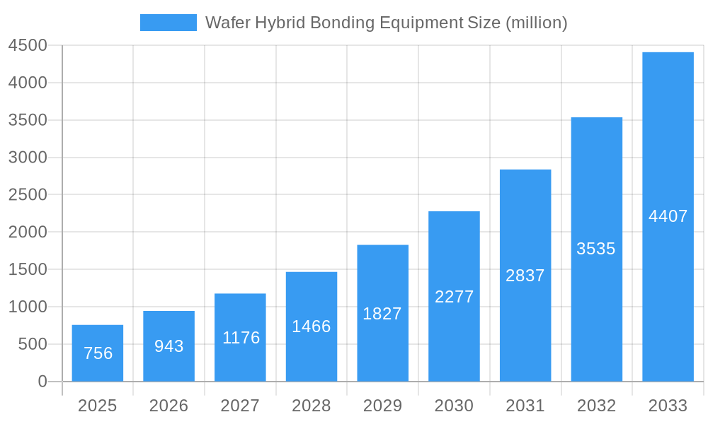
The Wafer Hybrid Bonding Equipment market is experiencing a period of robust expansion, projected to reach approximately $756 million by 2025. This impressive growth is fueled by a compound annual growth rate (CAGR) of 24.7%, indicating a dynamic and rapidly evolving industry. The primary drivers behind this surge include the escalating demand for advanced semiconductor devices, particularly in the realm of CMOS Image Sensors (CIS) for smartphones and automotive applications, and the burgeoning need for higher memory densities and performance, evident in the growth of NAND and DRAM technologies. Furthermore, the increasing adoption of High Bandwidth Memory (HBM) in high-performance computing, AI, and data centers is a significant catalyst. Hybrid bonding, with its ability to enable finer interconnects and higher integration levels, is becoming indispensable for meeting the performance and miniaturization requirements of these cutting-edge applications.
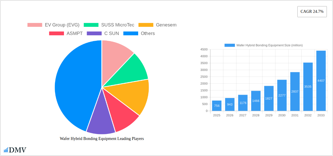
Wafer Hybrid Bonding Equipment Market Size (In Million)
The market is segmented into two key types of hybrid bonding: Wafer-to-wafer (W2W) hybrid bonding and Die-to-wafer (D2W) hybrid bonding. W2W bonding offers higher integration density for applications like stacked image sensors and 3D NAND, while D2W bonding provides flexibility for heterogeneous integration, such as combining different chip technologies. Key players like EV Group (EVG), SUSS MicroTec, and ASMPT are at the forefront, innovating and expanding their product portfolios to cater to the diverse needs of the semiconductor industry. Emerging players and regional advancements, particularly in Asia Pacific, are also contributing to market competition and technological evolution. Despite the strong growth trajectory, potential restraints could include the high capital expenditure required for advanced hybrid bonding equipment and the need for highly skilled personnel for operation and maintenance. However, the pervasive trend towards miniaturization, increased functionality, and energy efficiency in electronic devices continues to propel the demand for hybrid bonding solutions.
Wafer Hybrid Bonding Equipment Company Market Share
This comprehensive report offers an in-depth analysis of the Wafer Hybrid Bonding Equipment market, a critical technology driving advancements in semiconductor manufacturing. Explore the intricate landscape of wafer-to-wafer hybrid bonding and die-to-wafer hybrid bonding, essential for next-generation memory, logic, and sensing applications. Delve into the market's trajectory from 2019 to 2033, with a focus on the base year 2025 and a robust forecast period of 2025–2033.
Wafer Hybrid Bonding Equipment Market Composition & Trends
The Wafer Hybrid Bonding Equipment market exhibits a dynamic yet moderately concentrated landscape, with key players like EV Group (EVG), SUSS MicroTec, and ASMPT holding significant influence. Innovation remains a primary catalyst, driven by relentless demand for higher performance and miniaturization in sectors such as CMOS Image Sensor (CIS), NAND, DRAM, and High Bandwidth Memory (HBM). The regulatory environment, while generally supportive of semiconductor advancements, can introduce compliance considerations for new equipment. Substitute products, while present in less advanced interconnection technologies, are increasingly being outpaced by the superior density and performance offered by hybrid bonding. End-user profiles are diverse, ranging from leading semiconductor manufacturers to specialized foundries. Mergers and acquisitions (M&A) activity, estimated to be in the hundreds of millions, plays a crucial role in market consolidation and technology integration. For instance, estimated M&A deal values in the historical period (2019-2024) reached approximately 500 million.
- Market Share Distribution: Leading players account for an estimated 70% of the market share.
- Innovation Drivers: Miniaturization, performance enhancement, and power efficiency are paramount.
- Regulatory Impact: Emerging standards for advanced packaging and material safety influence equipment design.
- End-User Focus: High-volume manufacturing of advanced memory and logic devices.
- M&A Valuations: Significant investment in acquiring advanced hybrid bonding technologies and market access.
Wafer Hybrid Bonding Equipment Industry Evolution
The Wafer Hybrid Bonding Equipment industry has witnessed exponential growth and transformative evolution. From its nascent stages in the historical period (2019–2024), the market has matured significantly, propelled by groundbreaking technological advancements and a discernible shift in consumer demand towards devices with enhanced capabilities. The adoption of hybrid bonding technology has accelerated, driven by its unique ability to achieve near-zero interconnect pitch, thereby enabling unprecedented levels of integration and performance. This evolution is characterized by a compound annual growth rate (CAGR) estimated at a robust 25% during the forecast period (2025–2033). The increasing complexity of semiconductor architectures, particularly in High Bandwidth Memory (HBM) and advanced CMOS Image Sensors (CIS), has created an insatiable demand for the dense and efficient interconnectivity that wafer hybrid bonding provides. Furthermore, the transition towards more power-efficient and compact electronic devices has further cemented the position of hybrid bonding as a cornerstone technology for the future. The industry's capacity to innovate, adapt to new material science challenges, and scale manufacturing processes has been instrumental in its upward trajectory. The estimated market size in the base year 2025 is projected to reach 8,000 million.
Leading Regions, Countries, or Segments in Wafer Hybrid Bonding Equipment
The Wafer Hybrid Bonding Equipment market is currently dominated by regions and specific segments at the forefront of advanced semiconductor manufacturing. East Asia, particularly Taiwan and South Korea, stands out as the leading region due to its substantial concentration of foundries and memory manufacturers driving the adoption of cutting-edge packaging technologies. Within this region, significant investment trends and supportive government policies have created a fertile ground for hybrid bonding equipment. The wafer-to-wafer hybrid bonding segment, specifically for High Bandwidth Memory (HBM) and advanced CMOS Image Sensor (CIS) applications, exhibits the strongest dominance. The insatiable demand for higher performance and greater data transfer rates in AI accelerators, advanced graphics cards, and next-generation mobile devices directly fuels the adoption of HBM. Similarly, the continuous pursuit of higher resolution and enhanced imaging capabilities in smartphones and automotive applications drives the demand for advanced CIS, which benefits immensely from hybrid bonding for stacked sensor architectures.
- Dominant Region: East Asia (Taiwan, South Korea)
- Key Drivers: High concentration of leading foundries and memory manufacturers, substantial government R&D investment, favorable industrial policies, and a robust ecosystem for semiconductor innovation.
- Investment Trends: Billions invested annually in advanced packaging capabilities, including hybrid bonding.
- Regulatory Support: Government initiatives promoting domestic semiconductor manufacturing and technological self-sufficiency.
- Dominant Application Segment: High Bandwidth Memory (HBM) and CMOS Image Sensor (CIS)
- Dominance Factors for HBM: Critical for AI, high-performance computing, and gaming, requiring massive data throughput and low latency. Hybrid bonding enables the stacking of multiple DRAM dies with minimal signal loss.
- Dominance Factors for CIS: Essential for advanced smartphone cameras, automotive imaging, and surveillance systems. Hybrid bonding facilitates the integration of sensor and logic layers, improving image quality and reducing form factor.
- Dominant Type: Wafer-to-wafer Hybrid Bonding
- Rationale: Offers the highest potential for parallelism, throughput, and yield for high-volume production of stacked chiplets and memory.
Wafer Hybrid Bonding Equipment Product Innovations
Product innovations in Wafer Hybrid Bonding Equipment are focused on enhancing precision, throughput, and yield for complex interconnectivity. Leading manufacturers are developing equipment capable of achieving sub-micron alignment accuracy and unprecedented bonding force control, crucial for delicate wafer stacking. Advancements include sophisticated plasma activation techniques for surface preparation, enabling reliable low-temperature bonding. Furthermore, the integration of advanced in-situ metrology and inspection systems ensures real-time process monitoring and defect detection, significantly improving overall yield. These innovations are directly enabling breakthroughs in CMOS Image Sensor (CIS) with higher pixel densities and enhanced low-light performance, as well as denser and faster NAND and DRAM architectures, including next-generation High Bandwidth Memory (HBM). The estimated total market value for these innovative solutions is projected to reach 15,000 million by 2033.
Propelling Factors for Wafer Hybrid Bonding Equipment Growth
The growth of the Wafer Hybrid Bonding Equipment market is primarily propelled by an escalating demand for higher semiconductor performance and increased functionality. The relentless drive for miniaturization across consumer electronics, automotive, and data center applications necessitates advanced packaging solutions like hybrid bonding. Technological advancements in wafer thinning, CMP, and metrology are enabling more complex and higher-density interconnects. Economically, the increasing value proposition of high-performance computing and AI workloads justifies the investment in sophisticated bonding equipment. Regulatory support for semiconductor innovation and domestic manufacturing also plays a significant role, encouraging adoption and R&D.
Obstacles in the Wafer Hybrid Bonding Equipment Market
Despite its immense potential, the Wafer Hybrid Bonding Equipment market faces several obstacles. High capital expenditure for advanced equipment presents a significant barrier to entry for smaller players. Complex process integration and the need for highly skilled labor can lead to manufacturing challenges and potential supply chain disruptions, impacting production timelines. Furthermore, evolving material requirements and the stringent quality control demanded for high-yield bonding processes require continuous investment in R&D and process optimization. The market for this specialized equipment is estimated at approximately 2,000 million in the base year 2025.
Future Opportunities in Wafer Hybrid Bonding Equipment
Emerging opportunities in the Wafer Hybrid Bonding Equipment market are abundant, driven by the burgeoning fields of AI, advanced computing, and 3D integration. The expansion of High Bandwidth Memory (HBM) applications into new domains like edge AI and autonomous systems presents a significant growth avenue. Furthermore, the development of novel materials and bonding techniques promises to unlock new possibilities for heterogeneous integration, enabling the creation of highly specialized and powerful System-in-Package (SiP) solutions. The growing demand for advanced CMOS Image Sensors (CIS) in emerging markets like augmented reality (AR) and virtual reality (VR) also offers substantial expansion potential. The total market value is projected to reach 15,000 million by 2033.
Major Players in the Wafer Hybrid Bonding Equipment Ecosystem
- EV Group (EVG)
- SUSS MicroTec
- Genesem
- ASMPT
- C SUN
- Piotech
- Beijing U-Precision Tech
- Wisdom Semiconductor Technology
Key Developments in Wafer Hybrid Bonding Equipment Industry
- 2023 Q3: EV Group launches an advanced hybrid bonding system with enhanced alignment accuracy for advanced packaging applications.
- 2023 Q4: ASMPT announces a strategic partnership to accelerate the development of die-to-wafer hybrid bonding solutions for next-generation memory.
- 2024 Q1: SUSS MicroTec showcases a new plasma activation technology significantly improving bond reliability for wafer hybrid bonding.
- 2024 Q2: Piotech demonstrates breakthrough results in low-temperature hybrid bonding for sensitive stacked image sensors.
- 2024 Q3: Genesem reports on the successful integration of hybrid bonding into high-volume manufacturing for advanced DRAM.
- 2024 Q4: Wisdom Semiconductor Technology announces a new manufacturing process enabling higher throughput for wafer-to-wafer hybrid bonding.
- 2025 Q1 (Projected): Beijing U-Precision Tech to unveil a next-generation metrology solution for hybrid bonding process control.
Strategic Wafer Hybrid Bonding Equipment Market Forecast
The strategic forecast for the Wafer Hybrid Bonding Equipment market is overwhelmingly positive, driven by the indispensable role of this technology in enabling future semiconductor advancements. The sustained demand for higher performance in AI, data centers, and advanced consumer electronics will continue to fuel the adoption of wafer-to-wafer hybrid bonding and die-to-wafer hybrid bonding. Key growth catalysts include the ongoing innovation in High Bandwidth Memory (HBM) and CMOS Image Sensors (CIS), alongside the exploration of novel applications in areas like advanced packaging for artificial intelligence and automotive systems. The market is poised for substantial growth, with the total market value projected to reach an impressive 15,000 million by 2033, highlighting its critical importance in the semiconductor value chain.
Wafer Hybrid Bonding Equipment Segmentation
-
1. Application
- 1.1. CMOS Image Sensor (CIS)
- 1.2. NAND
- 1.3. DRAM
- 1.4. High Bandwidth Memory (HBM)
- 1.5. Others
-
2. Type
- 2.1. Wafer-to-wafer Hybrid Bonding
- 2.2. Die-to-wafer Hybrid Bonding
Wafer Hybrid Bonding Equipment Segmentation By Geography
-
1. North America
- 1.1. United States
- 1.2. Canada
- 1.3. Mexico
-
2. South America
- 2.1. Brazil
- 2.2. Argentina
- 2.3. Rest of South America
-
3. Europe
- 3.1. United Kingdom
- 3.2. Germany
- 3.3. France
- 3.4. Italy
- 3.5. Spain
- 3.6. Russia
- 3.7. Benelux
- 3.8. Nordics
- 3.9. Rest of Europe
-
4. Middle East & Africa
- 4.1. Turkey
- 4.2. Israel
- 4.3. GCC
- 4.4. North Africa
- 4.5. South Africa
- 4.6. Rest of Middle East & Africa
-
5. Asia Pacific
- 5.1. China
- 5.2. India
- 5.3. Japan
- 5.4. South Korea
- 5.5. ASEAN
- 5.6. Oceania
- 5.7. Rest of Asia Pacific
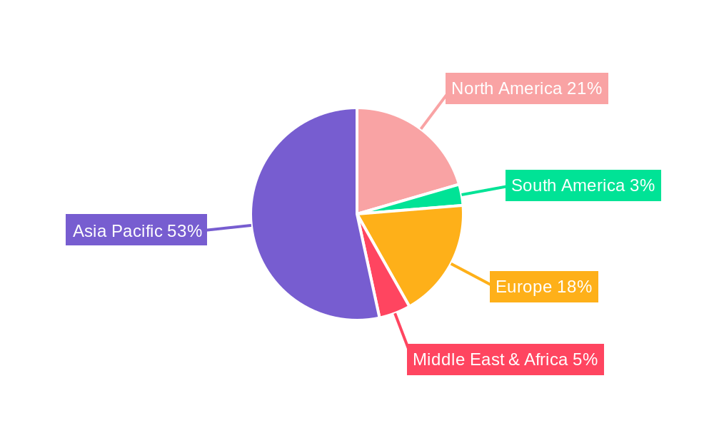
Wafer Hybrid Bonding Equipment Regional Market Share
Geographic Coverage of Wafer Hybrid Bonding Equipment
Wafer Hybrid Bonding Equipment REPORT HIGHLIGHTS
| Aspects | Details |
|---|---|
| Study Period | 2020-2034 |
| Base Year | 2025 |
| Estimated Year | 2026 |
| Forecast Period | 2026-2034 |
| Historical Period | 2020-2025 |
| Growth Rate | CAGR of 5.4% from 2020-2034 |
| Segmentation |
|
Table of Contents
- 1. Introduction
- 1.1. Research Scope
- 1.2. Market Segmentation
- 1.3. Research Objective
- 1.4. Definitions and Assumptions
- 2. Executive Summary
- 2.1. Market Snapshot
- 3. Market Dynamics
- 3.1. Market Drivers
- 3.2. Market Restrains
- 3.3. Market Trends
- 3.4. Market Opportunities
- 4. Market Factor Analysis
- 4.1. Porters Five Forces
- 4.1.1. Bargaining Power of Suppliers
- 4.1.2. Bargaining Power of Buyers
- 4.1.3. Threat of New Entrants
- 4.1.4. Threat of Substitutes
- 4.1.5. Competitive Rivalry
- 4.2. PESTEL analysis
- 4.3. BCG Analysis
- 4.3.1. Stars (High Growth, High Market Share)
- 4.3.2. Cash Cows (Low Growth, High Market Share)
- 4.3.3. Question Mark (High Growth, Low Market Share)
- 4.3.4. Dogs (Low Growth, Low Market Share)
- 4.4. Ansoff Matrix Analysis
- 4.5. Supply Chain Analysis
- 4.6. Regulatory Landscape
- 4.7. Current Market Potential and Opportunity Assessment (TAM–SAM–SOM Framework)
- 4.8. DMV Analyst Note
- 4.1. Porters Five Forces
- 5. Market Analysis, Insights and Forecast 2021-2033
- 5.1. Market Analysis, Insights and Forecast - by Application
- 5.1.1. CMOS Image Sensor (CIS)
- 5.1.2. NAND
- 5.1.3. DRAM
- 5.1.4. High Bandwidth Memory (HBM)
- 5.1.5. Others
- 5.2. Market Analysis, Insights and Forecast - by Type
- 5.2.1. Wafer-to-wafer Hybrid Bonding
- 5.2.2. Die-to-wafer Hybrid Bonding
- 5.3. Market Analysis, Insights and Forecast - by Region
- 5.3.1. North America
- 5.3.2. South America
- 5.3.3. Europe
- 5.3.4. Middle East & Africa
- 5.3.5. Asia Pacific
- 5.1. Market Analysis, Insights and Forecast - by Application
- 6. Global Wafer Hybrid Bonding Equipment Analysis, Insights and Forecast, 2021-2033
- 6.1. Market Analysis, Insights and Forecast - by Application
- 6.1.1. CMOS Image Sensor (CIS)
- 6.1.2. NAND
- 6.1.3. DRAM
- 6.1.4. High Bandwidth Memory (HBM)
- 6.1.5. Others
- 6.2. Market Analysis, Insights and Forecast - by Type
- 6.2.1. Wafer-to-wafer Hybrid Bonding
- 6.2.2. Die-to-wafer Hybrid Bonding
- 6.1. Market Analysis, Insights and Forecast - by Application
- 7. North America Wafer Hybrid Bonding Equipment Analysis, Insights and Forecast, 2020-2032
- 7.1. Market Analysis, Insights and Forecast - by Application
- 7.1.1. CMOS Image Sensor (CIS)
- 7.1.2. NAND
- 7.1.3. DRAM
- 7.1.4. High Bandwidth Memory (HBM)
- 7.1.5. Others
- 7.2. Market Analysis, Insights and Forecast - by Type
- 7.2.1. Wafer-to-wafer Hybrid Bonding
- 7.2.2. Die-to-wafer Hybrid Bonding
- 7.1. Market Analysis, Insights and Forecast - by Application
- 8. South America Wafer Hybrid Bonding Equipment Analysis, Insights and Forecast, 2020-2032
- 8.1. Market Analysis, Insights and Forecast - by Application
- 8.1.1. CMOS Image Sensor (CIS)
- 8.1.2. NAND
- 8.1.3. DRAM
- 8.1.4. High Bandwidth Memory (HBM)
- 8.1.5. Others
- 8.2. Market Analysis, Insights and Forecast - by Type
- 8.2.1. Wafer-to-wafer Hybrid Bonding
- 8.2.2. Die-to-wafer Hybrid Bonding
- 8.1. Market Analysis, Insights and Forecast - by Application
- 9. Europe Wafer Hybrid Bonding Equipment Analysis, Insights and Forecast, 2020-2032
- 9.1. Market Analysis, Insights and Forecast - by Application
- 9.1.1. CMOS Image Sensor (CIS)
- 9.1.2. NAND
- 9.1.3. DRAM
- 9.1.4. High Bandwidth Memory (HBM)
- 9.1.5. Others
- 9.2. Market Analysis, Insights and Forecast - by Type
- 9.2.1. Wafer-to-wafer Hybrid Bonding
- 9.2.2. Die-to-wafer Hybrid Bonding
- 9.1. Market Analysis, Insights and Forecast - by Application
- 10. Middle East & Africa Wafer Hybrid Bonding Equipment Analysis, Insights and Forecast, 2020-2032
- 10.1. Market Analysis, Insights and Forecast - by Application
- 10.1.1. CMOS Image Sensor (CIS)
- 10.1.2. NAND
- 10.1.3. DRAM
- 10.1.4. High Bandwidth Memory (HBM)
- 10.1.5. Others
- 10.2. Market Analysis, Insights and Forecast - by Type
- 10.2.1. Wafer-to-wafer Hybrid Bonding
- 10.2.2. Die-to-wafer Hybrid Bonding
- 10.1. Market Analysis, Insights and Forecast - by Application
- 11. Asia Pacific Wafer Hybrid Bonding Equipment Analysis, Insights and Forecast, 2020-2032
- 11.1. Market Analysis, Insights and Forecast - by Application
- 11.1.1. CMOS Image Sensor (CIS)
- 11.1.2. NAND
- 11.1.3. DRAM
- 11.1.4. High Bandwidth Memory (HBM)
- 11.1.5. Others
- 11.2. Market Analysis, Insights and Forecast - by Type
- 11.2.1. Wafer-to-wafer Hybrid Bonding
- 11.2.2. Die-to-wafer Hybrid Bonding
- 11.1. Market Analysis, Insights and Forecast - by Application
- 12. Competitive Analysis
- 12.1. Company Profiles
- 12.1.1 EV Group (EVG)
- 12.1.1.1. Company Overview
- 12.1.1.2. Products
- 12.1.1.3. Company Financials
- 12.1.1.4. SWOT Analysis
- 12.1.2 SUSS MicroTec
- 12.1.2.1. Company Overview
- 12.1.2.2. Products
- 12.1.2.3. Company Financials
- 12.1.2.4. SWOT Analysis
- 12.1.3 Genesem
- 12.1.3.1. Company Overview
- 12.1.3.2. Products
- 12.1.3.3. Company Financials
- 12.1.3.4. SWOT Analysis
- 12.1.4 ASMPT
- 12.1.4.1. Company Overview
- 12.1.4.2. Products
- 12.1.4.3. Company Financials
- 12.1.4.4. SWOT Analysis
- 12.1.5 C SUN
- 12.1.5.1. Company Overview
- 12.1.5.2. Products
- 12.1.5.3. Company Financials
- 12.1.5.4. SWOT Analysis
- 12.1.6 Piotech
- 12.1.6.1. Company Overview
- 12.1.6.2. Products
- 12.1.6.3. Company Financials
- 12.1.6.4. SWOT Analysis
- 12.1.7 Beijing U-Precision Tech
- 12.1.7.1. Company Overview
- 12.1.7.2. Products
- 12.1.7.3. Company Financials
- 12.1.7.4. SWOT Analysis
- 12.1.8 Wisdom Semiconductor Technology
- 12.1.8.1. Company Overview
- 12.1.8.2. Products
- 12.1.8.3. Company Financials
- 12.1.8.4. SWOT Analysis
- 12.1.1 EV Group (EVG)
- 12.2. Market Entropy
- 12.2.1 Company's Key Areas Served
- 12.2.2 Recent Developments
- 12.3. Company Market Share Analysis 2025
- 12.3.1 Top 5 Companies Market Share Analysis
- 12.3.2 Top 3 Companies Market Share Analysis
- 12.4. List of Potential Customers
- 13. Research Methodology
List of Figures
- Figure 1: Global Wafer Hybrid Bonding Equipment Revenue Breakdown (undefined, %) by Region 2025 & 2033
- Figure 2: Global Wafer Hybrid Bonding Equipment Volume Breakdown (K, %) by Region 2025 & 2033
- Figure 3: North America Wafer Hybrid Bonding Equipment Revenue (undefined), by Application 2025 & 2033
- Figure 4: North America Wafer Hybrid Bonding Equipment Volume (K), by Application 2025 & 2033
- Figure 5: North America Wafer Hybrid Bonding Equipment Revenue Share (%), by Application 2025 & 2033
- Figure 6: North America Wafer Hybrid Bonding Equipment Volume Share (%), by Application 2025 & 2033
- Figure 7: North America Wafer Hybrid Bonding Equipment Revenue (undefined), by Type 2025 & 2033
- Figure 8: North America Wafer Hybrid Bonding Equipment Volume (K), by Type 2025 & 2033
- Figure 9: North America Wafer Hybrid Bonding Equipment Revenue Share (%), by Type 2025 & 2033
- Figure 10: North America Wafer Hybrid Bonding Equipment Volume Share (%), by Type 2025 & 2033
- Figure 11: North America Wafer Hybrid Bonding Equipment Revenue (undefined), by Country 2025 & 2033
- Figure 12: North America Wafer Hybrid Bonding Equipment Volume (K), by Country 2025 & 2033
- Figure 13: North America Wafer Hybrid Bonding Equipment Revenue Share (%), by Country 2025 & 2033
- Figure 14: North America Wafer Hybrid Bonding Equipment Volume Share (%), by Country 2025 & 2033
- Figure 15: South America Wafer Hybrid Bonding Equipment Revenue (undefined), by Application 2025 & 2033
- Figure 16: South America Wafer Hybrid Bonding Equipment Volume (K), by Application 2025 & 2033
- Figure 17: South America Wafer Hybrid Bonding Equipment Revenue Share (%), by Application 2025 & 2033
- Figure 18: South America Wafer Hybrid Bonding Equipment Volume Share (%), by Application 2025 & 2033
- Figure 19: South America Wafer Hybrid Bonding Equipment Revenue (undefined), by Type 2025 & 2033
- Figure 20: South America Wafer Hybrid Bonding Equipment Volume (K), by Type 2025 & 2033
- Figure 21: South America Wafer Hybrid Bonding Equipment Revenue Share (%), by Type 2025 & 2033
- Figure 22: South America Wafer Hybrid Bonding Equipment Volume Share (%), by Type 2025 & 2033
- Figure 23: South America Wafer Hybrid Bonding Equipment Revenue (undefined), by Country 2025 & 2033
- Figure 24: South America Wafer Hybrid Bonding Equipment Volume (K), by Country 2025 & 2033
- Figure 25: South America Wafer Hybrid Bonding Equipment Revenue Share (%), by Country 2025 & 2033
- Figure 26: South America Wafer Hybrid Bonding Equipment Volume Share (%), by Country 2025 & 2033
- Figure 27: Europe Wafer Hybrid Bonding Equipment Revenue (undefined), by Application 2025 & 2033
- Figure 28: Europe Wafer Hybrid Bonding Equipment Volume (K), by Application 2025 & 2033
- Figure 29: Europe Wafer Hybrid Bonding Equipment Revenue Share (%), by Application 2025 & 2033
- Figure 30: Europe Wafer Hybrid Bonding Equipment Volume Share (%), by Application 2025 & 2033
- Figure 31: Europe Wafer Hybrid Bonding Equipment Revenue (undefined), by Type 2025 & 2033
- Figure 32: Europe Wafer Hybrid Bonding Equipment Volume (K), by Type 2025 & 2033
- Figure 33: Europe Wafer Hybrid Bonding Equipment Revenue Share (%), by Type 2025 & 2033
- Figure 34: Europe Wafer Hybrid Bonding Equipment Volume Share (%), by Type 2025 & 2033
- Figure 35: Europe Wafer Hybrid Bonding Equipment Revenue (undefined), by Country 2025 & 2033
- Figure 36: Europe Wafer Hybrid Bonding Equipment Volume (K), by Country 2025 & 2033
- Figure 37: Europe Wafer Hybrid Bonding Equipment Revenue Share (%), by Country 2025 & 2033
- Figure 38: Europe Wafer Hybrid Bonding Equipment Volume Share (%), by Country 2025 & 2033
- Figure 39: Middle East & Africa Wafer Hybrid Bonding Equipment Revenue (undefined), by Application 2025 & 2033
- Figure 40: Middle East & Africa Wafer Hybrid Bonding Equipment Volume (K), by Application 2025 & 2033
- Figure 41: Middle East & Africa Wafer Hybrid Bonding Equipment Revenue Share (%), by Application 2025 & 2033
- Figure 42: Middle East & Africa Wafer Hybrid Bonding Equipment Volume Share (%), by Application 2025 & 2033
- Figure 43: Middle East & Africa Wafer Hybrid Bonding Equipment Revenue (undefined), by Type 2025 & 2033
- Figure 44: Middle East & Africa Wafer Hybrid Bonding Equipment Volume (K), by Type 2025 & 2033
- Figure 45: Middle East & Africa Wafer Hybrid Bonding Equipment Revenue Share (%), by Type 2025 & 2033
- Figure 46: Middle East & Africa Wafer Hybrid Bonding Equipment Volume Share (%), by Type 2025 & 2033
- Figure 47: Middle East & Africa Wafer Hybrid Bonding Equipment Revenue (undefined), by Country 2025 & 2033
- Figure 48: Middle East & Africa Wafer Hybrid Bonding Equipment Volume (K), by Country 2025 & 2033
- Figure 49: Middle East & Africa Wafer Hybrid Bonding Equipment Revenue Share (%), by Country 2025 & 2033
- Figure 50: Middle East & Africa Wafer Hybrid Bonding Equipment Volume Share (%), by Country 2025 & 2033
- Figure 51: Asia Pacific Wafer Hybrid Bonding Equipment Revenue (undefined), by Application 2025 & 2033
- Figure 52: Asia Pacific Wafer Hybrid Bonding Equipment Volume (K), by Application 2025 & 2033
- Figure 53: Asia Pacific Wafer Hybrid Bonding Equipment Revenue Share (%), by Application 2025 & 2033
- Figure 54: Asia Pacific Wafer Hybrid Bonding Equipment Volume Share (%), by Application 2025 & 2033
- Figure 55: Asia Pacific Wafer Hybrid Bonding Equipment Revenue (undefined), by Type 2025 & 2033
- Figure 56: Asia Pacific Wafer Hybrid Bonding Equipment Volume (K), by Type 2025 & 2033
- Figure 57: Asia Pacific Wafer Hybrid Bonding Equipment Revenue Share (%), by Type 2025 & 2033
- Figure 58: Asia Pacific Wafer Hybrid Bonding Equipment Volume Share (%), by Type 2025 & 2033
- Figure 59: Asia Pacific Wafer Hybrid Bonding Equipment Revenue (undefined), by Country 2025 & 2033
- Figure 60: Asia Pacific Wafer Hybrid Bonding Equipment Volume (K), by Country 2025 & 2033
- Figure 61: Asia Pacific Wafer Hybrid Bonding Equipment Revenue Share (%), by Country 2025 & 2033
- Figure 62: Asia Pacific Wafer Hybrid Bonding Equipment Volume Share (%), by Country 2025 & 2033
List of Tables
- Table 1: Global Wafer Hybrid Bonding Equipment Revenue undefined Forecast, by Application 2020 & 2033
- Table 2: Global Wafer Hybrid Bonding Equipment Volume K Forecast, by Application 2020 & 2033
- Table 3: Global Wafer Hybrid Bonding Equipment Revenue undefined Forecast, by Type 2020 & 2033
- Table 4: Global Wafer Hybrid Bonding Equipment Volume K Forecast, by Type 2020 & 2033
- Table 5: Global Wafer Hybrid Bonding Equipment Revenue undefined Forecast, by Region 2020 & 2033
- Table 6: Global Wafer Hybrid Bonding Equipment Volume K Forecast, by Region 2020 & 2033
- Table 7: Global Wafer Hybrid Bonding Equipment Revenue undefined Forecast, by Application 2020 & 2033
- Table 8: Global Wafer Hybrid Bonding Equipment Volume K Forecast, by Application 2020 & 2033
- Table 9: Global Wafer Hybrid Bonding Equipment Revenue undefined Forecast, by Type 2020 & 2033
- Table 10: Global Wafer Hybrid Bonding Equipment Volume K Forecast, by Type 2020 & 2033
- Table 11: Global Wafer Hybrid Bonding Equipment Revenue undefined Forecast, by Country 2020 & 2033
- Table 12: Global Wafer Hybrid Bonding Equipment Volume K Forecast, by Country 2020 & 2033
- Table 13: United States Wafer Hybrid Bonding Equipment Revenue (undefined) Forecast, by Application 2020 & 2033
- Table 14: United States Wafer Hybrid Bonding Equipment Volume (K) Forecast, by Application 2020 & 2033
- Table 15: Canada Wafer Hybrid Bonding Equipment Revenue (undefined) Forecast, by Application 2020 & 2033
- Table 16: Canada Wafer Hybrid Bonding Equipment Volume (K) Forecast, by Application 2020 & 2033
- Table 17: Mexico Wafer Hybrid Bonding Equipment Revenue (undefined) Forecast, by Application 2020 & 2033
- Table 18: Mexico Wafer Hybrid Bonding Equipment Volume (K) Forecast, by Application 2020 & 2033
- Table 19: Global Wafer Hybrid Bonding Equipment Revenue undefined Forecast, by Application 2020 & 2033
- Table 20: Global Wafer Hybrid Bonding Equipment Volume K Forecast, by Application 2020 & 2033
- Table 21: Global Wafer Hybrid Bonding Equipment Revenue undefined Forecast, by Type 2020 & 2033
- Table 22: Global Wafer Hybrid Bonding Equipment Volume K Forecast, by Type 2020 & 2033
- Table 23: Global Wafer Hybrid Bonding Equipment Revenue undefined Forecast, by Country 2020 & 2033
- Table 24: Global Wafer Hybrid Bonding Equipment Volume K Forecast, by Country 2020 & 2033
- Table 25: Brazil Wafer Hybrid Bonding Equipment Revenue (undefined) Forecast, by Application 2020 & 2033
- Table 26: Brazil Wafer Hybrid Bonding Equipment Volume (K) Forecast, by Application 2020 & 2033
- Table 27: Argentina Wafer Hybrid Bonding Equipment Revenue (undefined) Forecast, by Application 2020 & 2033
- Table 28: Argentina Wafer Hybrid Bonding Equipment Volume (K) Forecast, by Application 2020 & 2033
- Table 29: Rest of South America Wafer Hybrid Bonding Equipment Revenue (undefined) Forecast, by Application 2020 & 2033
- Table 30: Rest of South America Wafer Hybrid Bonding Equipment Volume (K) Forecast, by Application 2020 & 2033
- Table 31: Global Wafer Hybrid Bonding Equipment Revenue undefined Forecast, by Application 2020 & 2033
- Table 32: Global Wafer Hybrid Bonding Equipment Volume K Forecast, by Application 2020 & 2033
- Table 33: Global Wafer Hybrid Bonding Equipment Revenue undefined Forecast, by Type 2020 & 2033
- Table 34: Global Wafer Hybrid Bonding Equipment Volume K Forecast, by Type 2020 & 2033
- Table 35: Global Wafer Hybrid Bonding Equipment Revenue undefined Forecast, by Country 2020 & 2033
- Table 36: Global Wafer Hybrid Bonding Equipment Volume K Forecast, by Country 2020 & 2033
- Table 37: United Kingdom Wafer Hybrid Bonding Equipment Revenue (undefined) Forecast, by Application 2020 & 2033
- Table 38: United Kingdom Wafer Hybrid Bonding Equipment Volume (K) Forecast, by Application 2020 & 2033
- Table 39: Germany Wafer Hybrid Bonding Equipment Revenue (undefined) Forecast, by Application 2020 & 2033
- Table 40: Germany Wafer Hybrid Bonding Equipment Volume (K) Forecast, by Application 2020 & 2033
- Table 41: France Wafer Hybrid Bonding Equipment Revenue (undefined) Forecast, by Application 2020 & 2033
- Table 42: France Wafer Hybrid Bonding Equipment Volume (K) Forecast, by Application 2020 & 2033
- Table 43: Italy Wafer Hybrid Bonding Equipment Revenue (undefined) Forecast, by Application 2020 & 2033
- Table 44: Italy Wafer Hybrid Bonding Equipment Volume (K) Forecast, by Application 2020 & 2033
- Table 45: Spain Wafer Hybrid Bonding Equipment Revenue (undefined) Forecast, by Application 2020 & 2033
- Table 46: Spain Wafer Hybrid Bonding Equipment Volume (K) Forecast, by Application 2020 & 2033
- Table 47: Russia Wafer Hybrid Bonding Equipment Revenue (undefined) Forecast, by Application 2020 & 2033
- Table 48: Russia Wafer Hybrid Bonding Equipment Volume (K) Forecast, by Application 2020 & 2033
- Table 49: Benelux Wafer Hybrid Bonding Equipment Revenue (undefined) Forecast, by Application 2020 & 2033
- Table 50: Benelux Wafer Hybrid Bonding Equipment Volume (K) Forecast, by Application 2020 & 2033
- Table 51: Nordics Wafer Hybrid Bonding Equipment Revenue (undefined) Forecast, by Application 2020 & 2033
- Table 52: Nordics Wafer Hybrid Bonding Equipment Volume (K) Forecast, by Application 2020 & 2033
- Table 53: Rest of Europe Wafer Hybrid Bonding Equipment Revenue (undefined) Forecast, by Application 2020 & 2033
- Table 54: Rest of Europe Wafer Hybrid Bonding Equipment Volume (K) Forecast, by Application 2020 & 2033
- Table 55: Global Wafer Hybrid Bonding Equipment Revenue undefined Forecast, by Application 2020 & 2033
- Table 56: Global Wafer Hybrid Bonding Equipment Volume K Forecast, by Application 2020 & 2033
- Table 57: Global Wafer Hybrid Bonding Equipment Revenue undefined Forecast, by Type 2020 & 2033
- Table 58: Global Wafer Hybrid Bonding Equipment Volume K Forecast, by Type 2020 & 2033
- Table 59: Global Wafer Hybrid Bonding Equipment Revenue undefined Forecast, by Country 2020 & 2033
- Table 60: Global Wafer Hybrid Bonding Equipment Volume K Forecast, by Country 2020 & 2033
- Table 61: Turkey Wafer Hybrid Bonding Equipment Revenue (undefined) Forecast, by Application 2020 & 2033
- Table 62: Turkey Wafer Hybrid Bonding Equipment Volume (K) Forecast, by Application 2020 & 2033
- Table 63: Israel Wafer Hybrid Bonding Equipment Revenue (undefined) Forecast, by Application 2020 & 2033
- Table 64: Israel Wafer Hybrid Bonding Equipment Volume (K) Forecast, by Application 2020 & 2033
- Table 65: GCC Wafer Hybrid Bonding Equipment Revenue (undefined) Forecast, by Application 2020 & 2033
- Table 66: GCC Wafer Hybrid Bonding Equipment Volume (K) Forecast, by Application 2020 & 2033
- Table 67: North Africa Wafer Hybrid Bonding Equipment Revenue (undefined) Forecast, by Application 2020 & 2033
- Table 68: North Africa Wafer Hybrid Bonding Equipment Volume (K) Forecast, by Application 2020 & 2033
- Table 69: South Africa Wafer Hybrid Bonding Equipment Revenue (undefined) Forecast, by Application 2020 & 2033
- Table 70: South Africa Wafer Hybrid Bonding Equipment Volume (K) Forecast, by Application 2020 & 2033
- Table 71: Rest of Middle East & Africa Wafer Hybrid Bonding Equipment Revenue (undefined) Forecast, by Application 2020 & 2033
- Table 72: Rest of Middle East & Africa Wafer Hybrid Bonding Equipment Volume (K) Forecast, by Application 2020 & 2033
- Table 73: Global Wafer Hybrid Bonding Equipment Revenue undefined Forecast, by Application 2020 & 2033
- Table 74: Global Wafer Hybrid Bonding Equipment Volume K Forecast, by Application 2020 & 2033
- Table 75: Global Wafer Hybrid Bonding Equipment Revenue undefined Forecast, by Type 2020 & 2033
- Table 76: Global Wafer Hybrid Bonding Equipment Volume K Forecast, by Type 2020 & 2033
- Table 77: Global Wafer Hybrid Bonding Equipment Revenue undefined Forecast, by Country 2020 & 2033
- Table 78: Global Wafer Hybrid Bonding Equipment Volume K Forecast, by Country 2020 & 2033
- Table 79: China Wafer Hybrid Bonding Equipment Revenue (undefined) Forecast, by Application 2020 & 2033
- Table 80: China Wafer Hybrid Bonding Equipment Volume (K) Forecast, by Application 2020 & 2033
- Table 81: India Wafer Hybrid Bonding Equipment Revenue (undefined) Forecast, by Application 2020 & 2033
- Table 82: India Wafer Hybrid Bonding Equipment Volume (K) Forecast, by Application 2020 & 2033
- Table 83: Japan Wafer Hybrid Bonding Equipment Revenue (undefined) Forecast, by Application 2020 & 2033
- Table 84: Japan Wafer Hybrid Bonding Equipment Volume (K) Forecast, by Application 2020 & 2033
- Table 85: South Korea Wafer Hybrid Bonding Equipment Revenue (undefined) Forecast, by Application 2020 & 2033
- Table 86: South Korea Wafer Hybrid Bonding Equipment Volume (K) Forecast, by Application 2020 & 2033
- Table 87: ASEAN Wafer Hybrid Bonding Equipment Revenue (undefined) Forecast, by Application 2020 & 2033
- Table 88: ASEAN Wafer Hybrid Bonding Equipment Volume (K) Forecast, by Application 2020 & 2033
- Table 89: Oceania Wafer Hybrid Bonding Equipment Revenue (undefined) Forecast, by Application 2020 & 2033
- Table 90: Oceania Wafer Hybrid Bonding Equipment Volume (K) Forecast, by Application 2020 & 2033
- Table 91: Rest of Asia Pacific Wafer Hybrid Bonding Equipment Revenue (undefined) Forecast, by Application 2020 & 2033
- Table 92: Rest of Asia Pacific Wafer Hybrid Bonding Equipment Volume (K) Forecast, by Application 2020 & 2033
Frequently Asked Questions
1. What is the projected Compound Annual Growth Rate (CAGR) of the Wafer Hybrid Bonding Equipment?
The projected CAGR is approximately 5.4%.
2. Which companies are prominent players in the Wafer Hybrid Bonding Equipment?
Key companies in the market include EV Group (EVG), SUSS MicroTec, Genesem, ASMPT, C SUN, Piotech, Beijing U-Precision Tech, Wisdom Semiconductor Technology.
3. What are the main segments of the Wafer Hybrid Bonding Equipment?
The market segments include Application, Type.
4. Can you provide details about the market size?
The market size is estimated to be USD XXX N/A as of 2022.
5. What are some drivers contributing to market growth?
N/A
6. What are the notable trends driving market growth?
N/A
7. Are there any restraints impacting market growth?
N/A
8. Can you provide examples of recent developments in the market?
N/A
9. What pricing options are available for accessing the report?
Pricing options include single-user, multi-user, and enterprise licenses priced at USD 3950.00, USD 5925.00, and USD 7900.00 respectively.
10. Is the market size provided in terms of value or volume?
The market size is provided in terms of value, measured in N/A and volume, measured in K.
11. Are there any specific market keywords associated with the report?
Yes, the market keyword associated with the report is "Wafer Hybrid Bonding Equipment," which aids in identifying and referencing the specific market segment covered.
12. How do I determine which pricing option suits my needs best?
The pricing options vary based on user requirements and access needs. Individual users may opt for single-user licenses, while businesses requiring broader access may choose multi-user or enterprise licenses for cost-effective access to the report.
13. Are there any additional resources or data provided in the Wafer Hybrid Bonding Equipment report?
While the report offers comprehensive insights, it's advisable to review the specific contents or supplementary materials provided to ascertain if additional resources or data are available.
14. How can I stay updated on further developments or reports in the Wafer Hybrid Bonding Equipment?
To stay informed about further developments, trends, and reports in the Wafer Hybrid Bonding Equipment, consider subscribing to industry newsletters, following relevant companies and organizations, or regularly checking reputable industry news sources and publications.
Methodology
Step 1 - Identification of Relevant Samples Size from Population Database


Step 2 - Approaches for Defining Global Market Size (Value, Volume* & Price*)

Note*: In applicable scenarios
Step 3 - Data Sources
Primary Research
- Web Analytics
- Survey Reports
- Research Institute
- Latest Research Reports
- Opinion Leaders
Secondary Research
- Annual Reports
- White Paper
- Latest Press Release
- Industry Association
- Paid Database
- Investor Presentations

Step 4 - Data Triangulation
Involves using different sources of information in order to increase the validity of a study
These sources are likely to be stakeholders in a program - participants, other researchers, program staff, other community members, and so on.
Then we put all data in single framework & apply various statistical tools to find out the dynamic on the market.
During the analysis stage, feedback from the stakeholder groups would be compared to determine areas of agreement as well as areas of divergence