

Key Insights
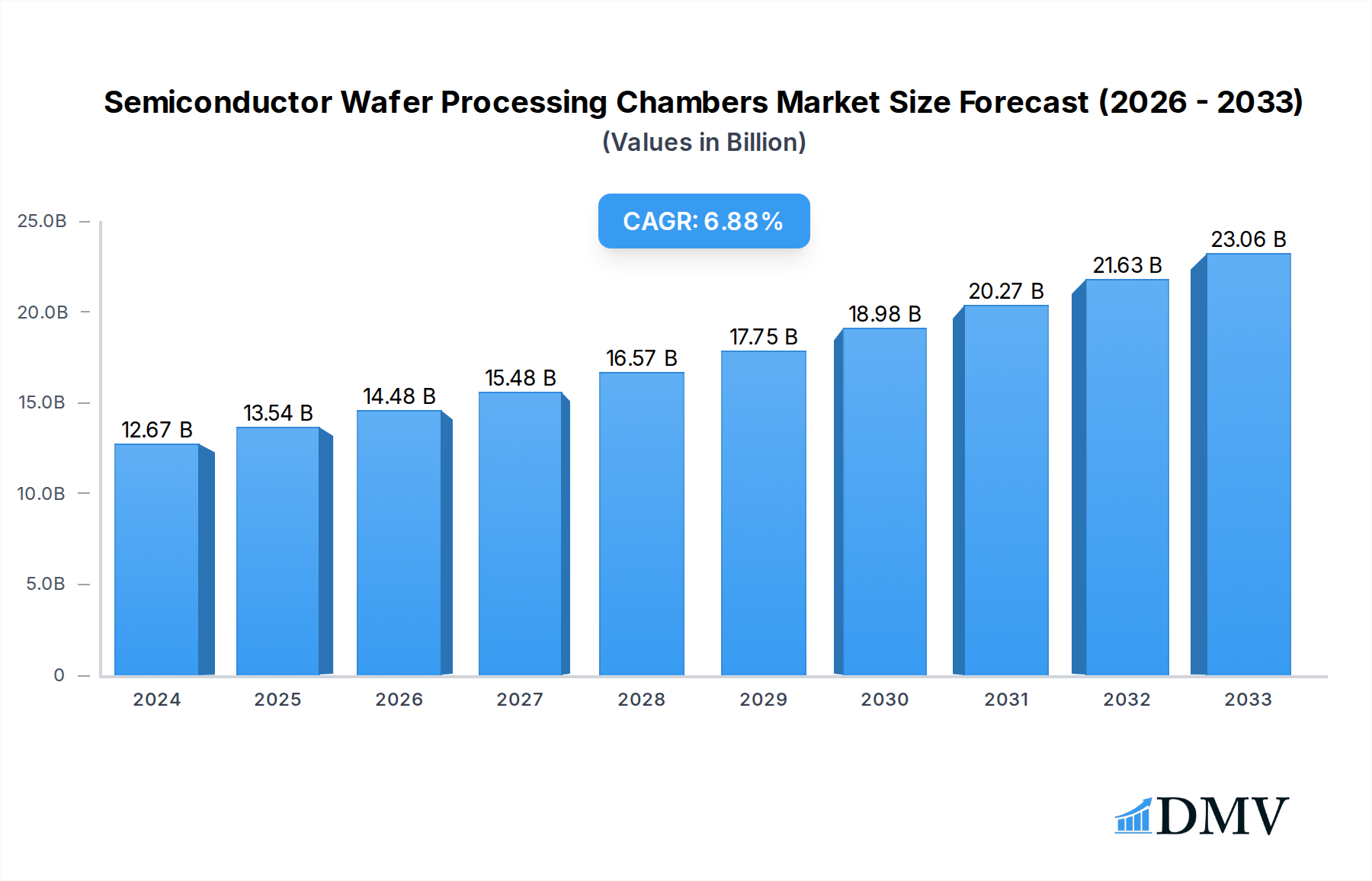
The global Semiconductor Wafer Processing Chambers market is poised for significant expansion, projected to reach $12.67 billion in 2024, with a robust Compound Annual Growth Rate (CAGR) of 6.8%. This upward trajectory is primarily fueled by the escalating demand for advanced semiconductor devices across various sectors, including artificial intelligence, 5G, automotive, and IoT. The relentless pursuit of smaller, more powerful, and energy-efficient chips necessitates sophisticated wafer processing techniques, directly driving the need for cutting-edge etching and thin-film deposition equipment, integral components of which are transition and reaction chambers. Emerging economies in the Asia Pacific region, particularly China and South Korea, are emerging as major hubs for semiconductor manufacturing, further stimulating market growth through increased investments in fabrication facilities and advanced R&D.

Semiconductor Wafer Processing Chambers Market Size (In Billion)
The market's dynamism is further underscored by the continuous innovation in chamber design and materials science aimed at enhancing process precision, yield, and throughput. Manufacturers are focusing on developing chambers capable of handling larger wafer sizes and supporting complex multi-step fabrication processes. While the market enjoys strong growth drivers, certain challenges persist. These include the high capital expenditure required for establishing and upgrading semiconductor fabrication plants, geopolitical tensions that can disrupt global supply chains, and the increasing complexity of wafer fabrication, demanding specialized expertise and advanced materials. Despite these restraints, the strategic importance of semiconductors in the modern digital economy, coupled with ongoing technological advancements, ensures a promising outlook for the Semiconductor Wafer Processing Chambers market. The competitive landscape is characterized by the presence of established global players and emerging regional manufacturers, all striving for market dominance through technological innovation and strategic collaborations.
Semiconductor Wafer Processing Chambers Company Market Share
This comprehensive report delves into the dynamic global market for Semiconductor Wafer Processing Chambers, offering in-depth analysis from 2019 to 2033. Covering critical aspects from market composition and trends to future growth opportunities, this study is an indispensable resource for stakeholders seeking to understand and capitalize on the evolution of semiconductor manufacturing technology. With a base year of 2025 and a forecast period extending to 2033, the report provides actionable intelligence for decision-makers across the semiconductor ecosystem.
Semiconductor Wafer Processing Chambers Market Composition & Trends
The global Semiconductor Wafer Processing Chambers market exhibits a moderately concentrated landscape, driven by significant R&D investments and increasing demand for advanced semiconductor devices. Innovation catalysts include the relentless pursuit of smaller process nodes, enhanced performance, and reduced manufacturing costs, necessitating sophisticated chamber designs for critical steps like etching and thin-film deposition. Regulatory landscapes, particularly concerning environmental standards and safety protocols within cleanroom environments, are also shaping chamber development and adoption. Substitute products, while less prevalent for core processing functions, are emerging in areas like advanced metrology and inspection integrated within processing flows. End-user profiles are dominated by integrated device manufacturers (IDMs) and foundries, with a growing interest from specialized chip developers. Mergers and acquisitions (M&A) activities are observed as key players consolidate capabilities and expand market reach. For instance, the total value of M&A deals in the semiconductor equipment sector has reached billions in recent years. Market share distribution is heavily influenced by technological leadership and the ability to cater to high-volume manufacturing requirements.
- Market Concentration: Moderately concentrated, with a few key players holding significant market share.
- Innovation Catalysts: Advanced node scaling, performance enhancement, cost reduction, emerging material science.
- Regulatory Landscapes: Environmental compliance, cleanroom standards, safety regulations.
- Substitute Products: Advanced metrology, integrated inspection systems.
- End-User Profiles: Integrated Device Manufacturers (IDMs), Foundries, fabless semiconductor companies.
- M&A Activities: Strategic acquisitions for technology integration and market expansion.
- M&A Deal Values: Billions of dollars in recent years within the broader semiconductor equipment sector.
Semiconductor Wafer Processing Chambers Industry Evolution
The semiconductor wafer processing chamber industry has witnessed a transformative evolution, characterized by a robust market growth trajectory fueled by the insatiable demand for advanced microelectronics. Over the historical period of 2019–2024, the market experienced steady expansion, with growth rates averaging approximately 8-10% annually, driven by the proliferation of smartphones, IoT devices, and burgeoning AI applications. The base year of 2025 stands as a pivotal point, with the market projected to continue its upward momentum, supported by massive global investments in semiconductor manufacturing capacity. Technological advancements have been the cornerstone of this evolution. The transition from older lithography techniques to advanced EUV lithography, for example, has demanded the development of highly specialized and precise wafer processing chambers capable of handling intricate deposition, etching, and cleaning processes with unprecedented accuracy. Thin-film deposition equipment has seen significant innovation, with atomic layer deposition (ALD) and chemical vapor deposition (CVD) technologies becoming more sophisticated, enabling the creation of ultra-thin, uniform films with precise material properties crucial for next-generation chip architectures. Similarly, etching equipment has advanced from wet etching to highly selective dry etching techniques, including plasma etching and reactive ion etching (RIE), to achieve sub-micron and nanometer-scale features with exceptional precision and control. Shifting consumer demands are also playing a crucial role. The ever-increasing need for higher processing power, lower energy consumption, and miniaturization in consumer electronics, automotive, and industrial applications directly translates into a demand for more advanced semiconductor devices, consequently driving the need for state-of-the-art wafer processing chambers. The adoption of AI and machine learning in chip design and manufacturing is further accelerating innovation, pushing the boundaries of what is achievable in terms of wafer processing complexity and efficiency. The market is projected to maintain a Compound Annual Growth Rate (CAGR) of around 9-11% during the forecast period of 2025–2033, signifying sustained and strong growth driven by these interconnected factors.
Leading Regions, Countries, or Segments in Semiconductor Wafer Processing Chambers
The dominance in the Semiconductor Wafer Processing Chambers market is multifaceted, with specific regions and segments emerging as key growth drivers and innovation hubs. From an application perspective, Etching Equipment and Thin Film Deposition Equipment represent the most significant segments, often comprising over 70% of the market value. These segments are critical for defining the intricate circuitry on semiconductor wafers, directly impacting device performance and functionality. Within these applications, Reaction Chambers play a pivotal role, being the core of processes like chemical vapor deposition (CVD), atomic layer deposition (ALD), and plasma-enhanced chemical vapor deposition (PECVD). Transition Chambers, while less dominant in volume, are crucial for maintaining process integrity between different fabrication steps. Geographically, East Asia, particularly Taiwan, South Korea, and China, leads the global market for semiconductor wafer processing chambers. This dominance is propelled by the presence of the world's largest foundries and integrated device manufacturers (IDMs) in these regions, coupled with substantial government investments in semiconductor self-sufficiency and technological advancement.
- Dominant Segments (Application):
- Etching Equipment: Essential for pattern transfer and feature creation, with high demand for advanced dry etching technologies. Key drivers include the need for sub-10nm feature sizes and increased wafer throughput.
- Thin Film Deposition Equipment: Critical for building complex device structures, with significant growth in ALD and advanced CVD techniques. Drivers include the demand for superior material properties, dielectric layers, and barrier films.
- Dominant Segments (Type):
- Reaction Chambers: The core of most wafer processing, encompassing CVD, ALD, Etch, and Lithography chambers. Growth is tied to the introduction of new materials and process chemistries.
- Transition Chambers: Vital for maintaining vacuum integrity and preventing cross-contamination, especially in multi-chamber cluster tools. Their importance escalates with increasingly complex wafer fab processes.
- Leading Regions:
- East Asia (Taiwan, South Korea, China): Characterized by massive foundry capacity, significant government support for domestic semiconductor industries, and a strong ecosystem of R&D and manufacturing. Investment trends are heavily skewed towards building new fabs and upgrading existing ones to support advanced nodes. Regulatory support for the semiconductor industry is robust, aiming for supply chain security and technological leadership. The sheer volume of wafer production in these regions makes them the primary consumers of processing chambers.
- North America: A strong hub for semiconductor R&D, design, and specialized manufacturing, with a growing emphasis on domestic production initiatives and advanced packaging technologies. Investment trends are focused on high-end R&D and niche manufacturing.
- Europe: Emerging as a significant player with renewed focus on domestic semiconductor production and innovation, particularly in automotive and industrial electronics. Investment trends are geared towards building new fabs and fostering collaboration across the value chain.
Semiconductor Wafer Processing Chambers Product Innovations
Product innovations in semiconductor wafer processing chambers are primarily focused on enhancing process precision, enabling new material integration, and improving throughput. Key advancements include the development of single-wafer processing chambers for critical deposition and etching steps, offering superior uniformity and process control compared to batch systems. Innovations in ALD technology, such as spatial ALD, are enabling faster deposition rates while maintaining atomic-level precision, crucial for advanced gate dielectrics and passivation layers. For etching, breakthroughs in plasma control and chamber design allow for highly anisotropic and selective etch profiles, essential for sub-5nm transistor fabrication. Performance metrics like wafer uniformity (achieving <0.5% variation across the wafer) and process repeatability are continuously being improved. Furthermore, chambers are increasingly incorporating in-situ metrology and real-time process monitoring capabilities to enable faster yield optimization and predictive maintenance.
Propelling Factors for Semiconductor Wafer Processing Chambers Growth
The growth of the semiconductor wafer processing chambers market is propelled by several interconnected factors. The relentless demand for more powerful and energy-efficient electronic devices across consumer electronics, automotive, telecommunications (5G/6G), and artificial intelligence fuels the need for advanced semiconductor manufacturing. Technological advancements, such as the transition to smaller process nodes (e.g., 3nm, 2nm, and beyond), necessitate highly sophisticated and precise wafer processing chambers for critical steps like advanced lithography, etching, and deposition. Government initiatives worldwide, aimed at boosting domestic semiconductor manufacturing capacity and ensuring supply chain resilience, are driving significant investments in new fab constructions and upgrades, directly translating into increased demand for processing equipment. The rapid adoption of technologies like AI, IoT, and autonomous driving further amplifies the need for specialized chips, requiring continuous innovation in wafer processing.
Obstacles in the Semiconductor Wafer Processing Chambers Market
Despite robust growth, the semiconductor wafer processing chambers market faces several obstacles. The immense capital expenditure required for setting up and maintaining state-of-the-art fabrication facilities can be a significant barrier, especially for emerging players. Stringent environmental regulations regarding chemical usage, waste disposal, and energy consumption in cleanroom environments necessitate ongoing compliance efforts and can increase operational costs. Global supply chain disruptions, exacerbated by geopolitical tensions and pandemics, can lead to delays in component sourcing and extended lead times for chamber delivery, impacting production schedules. Furthermore, the highly specialized nature of semiconductor manufacturing leads to intense competition among established players, requiring continuous innovation and competitive pricing strategies to maintain market share.
Future Opportunities in Semiconductor Wafer Processing Chambers
Emerging opportunities in the semiconductor wafer processing chambers market are vast and diversified. The growing demand for specialized chips in areas like high-performance computing (HPC), artificial intelligence accelerators, and advanced sensors presents a significant avenue for growth. The development and integration of new materials, such as 2D materials and advanced dielectrics, will require novel processing chamber designs and chemistries. The trend towards advanced packaging technologies, like chiplets and 3D stacking, opens up new opportunities for specialized processing equipment required in these intricate fabrication steps. Furthermore, the increasing focus on sustainable manufacturing practices will drive demand for energy-efficient and environmentally friendly processing chamber solutions. The expansion of semiconductor manufacturing into new geographic regions also presents significant market penetration opportunities.
Major Players in the Semiconductor Wafer Processing Chambers Ecosystem
- Shenyang Fortune Precision Equipment
- NMC
- Piotech Inc
- AMEC
- Ferrotec
- Beneq Group
- Beijing E-Town Semiconductor Technology
- Konfoong Materials International
- SPRINT PRECISION TECHNOLOGIES
- Tolerance Semiconductor Equipment Qidong
- Foxsemicon Integrated Technology
- Kunshan Kinglai Hygienic Materials
- Hwacheon
- Goodwill Precision Machinery
- Edwards
- Pfeiffer
- VATValve
Key Developments in Semiconductor Wafer Processing Chambers Industry
- 2024: Introduction of next-generation ALD chambers offering significantly faster deposition rates for advanced dielectrics.
- 2023: Launch of enhanced plasma etching chambers with superior selectivity for sub-3nm node manufacturing.
- 2022: Significant investments by major foundries in new wafer fab construction, boosting demand for all types of processing chambers.
- 2021: Increased focus on developing process chambers for advanced packaging technologies, including chiplet integration.
- 2020: Emergence of AI-driven process optimization in wafer processing chambers for improved yield and efficiency.
- 2019: Growing adoption of EUV lithography and associated processing equipment to support advanced node production.
Strategic Semiconductor Wafer Processing Chambers Market Forecast
The strategic forecast for the Semiconductor Wafer Processing Chambers market is exceptionally positive, driven by sustained technological advancements and the global imperative for enhanced semiconductor capabilities. The increasing complexity of chip architectures, coupled with the expansion of end-use applications into areas like AI, IoT, and automotive electronics, will continue to fuel demand for sophisticated etching and thin-film deposition equipment. Government support for domestic semiconductor manufacturing and the trend towards supply chain diversification further solidify the market's growth trajectory. Innovations in materials science and process integration will unlock new market segments and opportunities, particularly in advanced packaging and specialized semiconductor devices. The market is poised for robust expansion, presenting significant opportunities for companies that can offer cutting-edge, high-performance, and reliable wafer processing chamber solutions.
Semiconductor Wafer Processing Chambers Segmentation
-
1. Application
- 1.1. Etching Equipment
- 1.2. Thin Film Deposition Equipment
-
2. Type
- 2.1. Transition Chambers
- 2.2. Reaction Chambers
- 2.3. Others
Semiconductor Wafer Processing Chambers Segmentation By Geography
-
1. North America
- 1.1. United States
- 1.2. Canada
- 1.3. Mexico
-
2. South America
- 2.1. Brazil
- 2.2. Argentina
- 2.3. Rest of South America
-
3. Europe
- 3.1. United Kingdom
- 3.2. Germany
- 3.3. France
- 3.4. Italy
- 3.5. Spain
- 3.6. Russia
- 3.7. Benelux
- 3.8. Nordics
- 3.9. Rest of Europe
-
4. Middle East & Africa
- 4.1. Turkey
- 4.2. Israel
- 4.3. GCC
- 4.4. North Africa
- 4.5. South Africa
- 4.6. Rest of Middle East & Africa
-
5. Asia Pacific
- 5.1. China
- 5.2. India
- 5.3. Japan
- 5.4. South Korea
- 5.5. ASEAN
- 5.6. Oceania
- 5.7. Rest of Asia Pacific
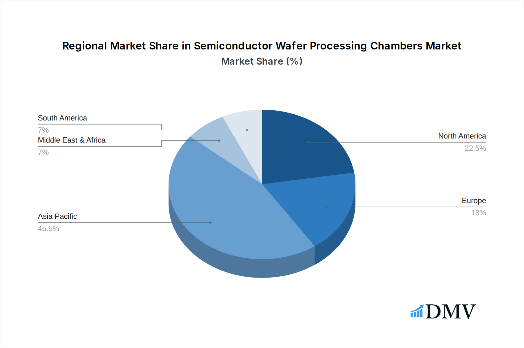
Semiconductor Wafer Processing Chambers Regional Market Share
Geographic Coverage of Semiconductor Wafer Processing Chambers
Semiconductor Wafer Processing Chambers REPORT HIGHLIGHTS
| Aspects | Details |
|---|---|
| Study Period | 2020-2034 |
| Base Year | 2025 |
| Estimated Year | 2026 |
| Forecast Period | 2026-2034 |
| Historical Period | 2020-2025 |
| Growth Rate | CAGR of 10.24% from 2020-2034 |
| Segmentation |
|
Table of Contents
- 1. Introduction
- 1.1. Research Scope
- 1.2. Market Segmentation
- 1.3. Research Objective
- 1.4. Definitions and Assumptions
- 2. Executive Summary
- 2.1. Market Snapshot
- 3. Market Dynamics
- 3.1. Market Drivers
- 3.2. Market Restrains
- 3.3. Market Trends
- 3.4. Market Opportunities
- 4. Market Factor Analysis
- 4.1. Porters Five Forces
- 4.1.1. Bargaining Power of Suppliers
- 4.1.2. Bargaining Power of Buyers
- 4.1.3. Threat of New Entrants
- 4.1.4. Threat of Substitutes
- 4.1.5. Competitive Rivalry
- 4.2. PESTEL analysis
- 4.3. BCG Analysis
- 4.3.1. Stars (High Growth, High Market Share)
- 4.3.2. Cash Cows (Low Growth, High Market Share)
- 4.3.3. Question Mark (High Growth, Low Market Share)
- 4.3.4. Dogs (Low Growth, Low Market Share)
- 4.4. Ansoff Matrix Analysis
- 4.5. Supply Chain Analysis
- 4.6. Regulatory Landscape
- 4.7. Current Market Potential and Opportunity Assessment (TAM–SAM–SOM Framework)
- 4.8. DMV Analyst Note
- 4.1. Porters Five Forces
- 5. Market Analysis, Insights and Forecast 2021-2033
- 5.1. Market Analysis, Insights and Forecast - by Application
- 5.1.1. Etching Equipment
- 5.1.2. Thin Film Deposition Equipment
- 5.2. Market Analysis, Insights and Forecast - by Type
- 5.2.1. Transition Chambers
- 5.2.2. Reaction Chambers
- 5.2.3. Others
- 5.3. Market Analysis, Insights and Forecast - by Region
- 5.3.1. North America
- 5.3.2. South America
- 5.3.3. Europe
- 5.3.4. Middle East & Africa
- 5.3.5. Asia Pacific
- 5.1. Market Analysis, Insights and Forecast - by Application
- 6. Global Semiconductor Wafer Processing Chambers Analysis, Insights and Forecast, 2021-2033
- 6.1. Market Analysis, Insights and Forecast - by Application
- 6.1.1. Etching Equipment
- 6.1.2. Thin Film Deposition Equipment
- 6.2. Market Analysis, Insights and Forecast - by Type
- 6.2.1. Transition Chambers
- 6.2.2. Reaction Chambers
- 6.2.3. Others
- 6.1. Market Analysis, Insights and Forecast - by Application
- 7. North America Semiconductor Wafer Processing Chambers Analysis, Insights and Forecast, 2020-2032
- 7.1. Market Analysis, Insights and Forecast - by Application
- 7.1.1. Etching Equipment
- 7.1.2. Thin Film Deposition Equipment
- 7.2. Market Analysis, Insights and Forecast - by Type
- 7.2.1. Transition Chambers
- 7.2.2. Reaction Chambers
- 7.2.3. Others
- 7.1. Market Analysis, Insights and Forecast - by Application
- 8. South America Semiconductor Wafer Processing Chambers Analysis, Insights and Forecast, 2020-2032
- 8.1. Market Analysis, Insights and Forecast - by Application
- 8.1.1. Etching Equipment
- 8.1.2. Thin Film Deposition Equipment
- 8.2. Market Analysis, Insights and Forecast - by Type
- 8.2.1. Transition Chambers
- 8.2.2. Reaction Chambers
- 8.2.3. Others
- 8.1. Market Analysis, Insights and Forecast - by Application
- 9. Europe Semiconductor Wafer Processing Chambers Analysis, Insights and Forecast, 2020-2032
- 9.1. Market Analysis, Insights and Forecast - by Application
- 9.1.1. Etching Equipment
- 9.1.2. Thin Film Deposition Equipment
- 9.2. Market Analysis, Insights and Forecast - by Type
- 9.2.1. Transition Chambers
- 9.2.2. Reaction Chambers
- 9.2.3. Others
- 9.1. Market Analysis, Insights and Forecast - by Application
- 10. Middle East & Africa Semiconductor Wafer Processing Chambers Analysis, Insights and Forecast, 2020-2032
- 10.1. Market Analysis, Insights and Forecast - by Application
- 10.1.1. Etching Equipment
- 10.1.2. Thin Film Deposition Equipment
- 10.2. Market Analysis, Insights and Forecast - by Type
- 10.2.1. Transition Chambers
- 10.2.2. Reaction Chambers
- 10.2.3. Others
- 10.1. Market Analysis, Insights and Forecast - by Application
- 11. Asia Pacific Semiconductor Wafer Processing Chambers Analysis, Insights and Forecast, 2020-2032
- 11.1. Market Analysis, Insights and Forecast - by Application
- 11.1.1. Etching Equipment
- 11.1.2. Thin Film Deposition Equipment
- 11.2. Market Analysis, Insights and Forecast - by Type
- 11.2.1. Transition Chambers
- 11.2.2. Reaction Chambers
- 11.2.3. Others
- 11.1. Market Analysis, Insights and Forecast - by Application
- 12. Competitive Analysis
- 12.1. Company Profiles
- 12.1.1 Shenyang Fortune Precision Equipment
- 12.1.1.1. Company Overview
- 12.1.1.2. Products
- 12.1.1.3. Company Financials
- 12.1.1.4. SWOT Analysis
- 12.1.2 NMC
- 12.1.2.1. Company Overview
- 12.1.2.2. Products
- 12.1.2.3. Company Financials
- 12.1.2.4. SWOT Analysis
- 12.1.3 Piotech Inc
- 12.1.3.1. Company Overview
- 12.1.3.2. Products
- 12.1.3.3. Company Financials
- 12.1.3.4. SWOT Analysis
- 12.1.4 AMEC
- 12.1.4.1. Company Overview
- 12.1.4.2. Products
- 12.1.4.3. Company Financials
- 12.1.4.4. SWOT Analysis
- 12.1.5 Ferrotec
- 12.1.5.1. Company Overview
- 12.1.5.2. Products
- 12.1.5.3. Company Financials
- 12.1.5.4. SWOT Analysis
- 12.1.6 Beneq Group
- 12.1.6.1. Company Overview
- 12.1.6.2. Products
- 12.1.6.3. Company Financials
- 12.1.6.4. SWOT Analysis
- 12.1.7 Beijing E-Town Semiconductor Technology
- 12.1.7.1. Company Overview
- 12.1.7.2. Products
- 12.1.7.3. Company Financials
- 12.1.7.4. SWOT Analysis
- 12.1.8 Konfoong Materials International
- 12.1.8.1. Company Overview
- 12.1.8.2. Products
- 12.1.8.3. Company Financials
- 12.1.8.4. SWOT Analysis
- 12.1.9 SPRINT PRECISION TECHNOLOGIES
- 12.1.9.1. Company Overview
- 12.1.9.2. Products
- 12.1.9.3. Company Financials
- 12.1.9.4. SWOT Analysis
- 12.1.10 Tolerance Semiconductor Equipment Qidong
- 12.1.10.1. Company Overview
- 12.1.10.2. Products
- 12.1.10.3. Company Financials
- 12.1.10.4. SWOT Analysis
- 12.1.11 Foxsemicon Integrated Technology
- 12.1.11.1. Company Overview
- 12.1.11.2. Products
- 12.1.11.3. Company Financials
- 12.1.11.4. SWOT Analysis
- 12.1.12 Kunshan Kinglai Hygienic Materials
- 12.1.12.1. Company Overview
- 12.1.12.2. Products
- 12.1.12.3. Company Financials
- 12.1.12.4. SWOT Analysis
- 12.1.13 Hwacheon
- 12.1.13.1. Company Overview
- 12.1.13.2. Products
- 12.1.13.3. Company Financials
- 12.1.13.4. SWOT Analysis
- 12.1.14 Goodwill Precision Machinery
- 12.1.14.1. Company Overview
- 12.1.14.2. Products
- 12.1.14.3. Company Financials
- 12.1.14.4. SWOT Analysis
- 12.1.15 Edwards
- 12.1.15.1. Company Overview
- 12.1.15.2. Products
- 12.1.15.3. Company Financials
- 12.1.15.4. SWOT Analysis
- 12.1.16 Pfeiffer
- 12.1.16.1. Company Overview
- 12.1.16.2. Products
- 12.1.16.3. Company Financials
- 12.1.16.4. SWOT Analysis
- 12.1.17 VATValve
- 12.1.17.1. Company Overview
- 12.1.17.2. Products
- 12.1.17.3. Company Financials
- 12.1.17.4. SWOT Analysis
- 12.1.1 Shenyang Fortune Precision Equipment
- 12.2. Market Entropy
- 12.2.1 Company's Key Areas Served
- 12.2.2 Recent Developments
- 12.3. Company Market Share Analysis 2025
- 12.3.1 Top 5 Companies Market Share Analysis
- 12.3.2 Top 3 Companies Market Share Analysis
- 12.4. List of Potential Customers
- 13. Research Methodology
List of Figures
- Figure 1: Global Semiconductor Wafer Processing Chambers Revenue Breakdown (undefined, %) by Region 2025 & 2033
- Figure 2: North America Semiconductor Wafer Processing Chambers Revenue (undefined), by Application 2025 & 2033
- Figure 3: North America Semiconductor Wafer Processing Chambers Revenue Share (%), by Application 2025 & 2033
- Figure 4: North America Semiconductor Wafer Processing Chambers Revenue (undefined), by Type 2025 & 2033
- Figure 5: North America Semiconductor Wafer Processing Chambers Revenue Share (%), by Type 2025 & 2033
- Figure 6: North America Semiconductor Wafer Processing Chambers Revenue (undefined), by Country 2025 & 2033
- Figure 7: North America Semiconductor Wafer Processing Chambers Revenue Share (%), by Country 2025 & 2033
- Figure 8: South America Semiconductor Wafer Processing Chambers Revenue (undefined), by Application 2025 & 2033
- Figure 9: South America Semiconductor Wafer Processing Chambers Revenue Share (%), by Application 2025 & 2033
- Figure 10: South America Semiconductor Wafer Processing Chambers Revenue (undefined), by Type 2025 & 2033
- Figure 11: South America Semiconductor Wafer Processing Chambers Revenue Share (%), by Type 2025 & 2033
- Figure 12: South America Semiconductor Wafer Processing Chambers Revenue (undefined), by Country 2025 & 2033
- Figure 13: South America Semiconductor Wafer Processing Chambers Revenue Share (%), by Country 2025 & 2033
- Figure 14: Europe Semiconductor Wafer Processing Chambers Revenue (undefined), by Application 2025 & 2033
- Figure 15: Europe Semiconductor Wafer Processing Chambers Revenue Share (%), by Application 2025 & 2033
- Figure 16: Europe Semiconductor Wafer Processing Chambers Revenue (undefined), by Type 2025 & 2033
- Figure 17: Europe Semiconductor Wafer Processing Chambers Revenue Share (%), by Type 2025 & 2033
- Figure 18: Europe Semiconductor Wafer Processing Chambers Revenue (undefined), by Country 2025 & 2033
- Figure 19: Europe Semiconductor Wafer Processing Chambers Revenue Share (%), by Country 2025 & 2033
- Figure 20: Middle East & Africa Semiconductor Wafer Processing Chambers Revenue (undefined), by Application 2025 & 2033
- Figure 21: Middle East & Africa Semiconductor Wafer Processing Chambers Revenue Share (%), by Application 2025 & 2033
- Figure 22: Middle East & Africa Semiconductor Wafer Processing Chambers Revenue (undefined), by Type 2025 & 2033
- Figure 23: Middle East & Africa Semiconductor Wafer Processing Chambers Revenue Share (%), by Type 2025 & 2033
- Figure 24: Middle East & Africa Semiconductor Wafer Processing Chambers Revenue (undefined), by Country 2025 & 2033
- Figure 25: Middle East & Africa Semiconductor Wafer Processing Chambers Revenue Share (%), by Country 2025 & 2033
- Figure 26: Asia Pacific Semiconductor Wafer Processing Chambers Revenue (undefined), by Application 2025 & 2033
- Figure 27: Asia Pacific Semiconductor Wafer Processing Chambers Revenue Share (%), by Application 2025 & 2033
- Figure 28: Asia Pacific Semiconductor Wafer Processing Chambers Revenue (undefined), by Type 2025 & 2033
- Figure 29: Asia Pacific Semiconductor Wafer Processing Chambers Revenue Share (%), by Type 2025 & 2033
- Figure 30: Asia Pacific Semiconductor Wafer Processing Chambers Revenue (undefined), by Country 2025 & 2033
- Figure 31: Asia Pacific Semiconductor Wafer Processing Chambers Revenue Share (%), by Country 2025 & 2033
List of Tables
- Table 1: Global Semiconductor Wafer Processing Chambers Revenue undefined Forecast, by Application 2020 & 2033
- Table 2: Global Semiconductor Wafer Processing Chambers Revenue undefined Forecast, by Type 2020 & 2033
- Table 3: Global Semiconductor Wafer Processing Chambers Revenue undefined Forecast, by Region 2020 & 2033
- Table 4: Global Semiconductor Wafer Processing Chambers Revenue undefined Forecast, by Application 2020 & 2033
- Table 5: Global Semiconductor Wafer Processing Chambers Revenue undefined Forecast, by Type 2020 & 2033
- Table 6: Global Semiconductor Wafer Processing Chambers Revenue undefined Forecast, by Country 2020 & 2033
- Table 7: United States Semiconductor Wafer Processing Chambers Revenue (undefined) Forecast, by Application 2020 & 2033
- Table 8: Canada Semiconductor Wafer Processing Chambers Revenue (undefined) Forecast, by Application 2020 & 2033
- Table 9: Mexico Semiconductor Wafer Processing Chambers Revenue (undefined) Forecast, by Application 2020 & 2033
- Table 10: Global Semiconductor Wafer Processing Chambers Revenue undefined Forecast, by Application 2020 & 2033
- Table 11: Global Semiconductor Wafer Processing Chambers Revenue undefined Forecast, by Type 2020 & 2033
- Table 12: Global Semiconductor Wafer Processing Chambers Revenue undefined Forecast, by Country 2020 & 2033
- Table 13: Brazil Semiconductor Wafer Processing Chambers Revenue (undefined) Forecast, by Application 2020 & 2033
- Table 14: Argentina Semiconductor Wafer Processing Chambers Revenue (undefined) Forecast, by Application 2020 & 2033
- Table 15: Rest of South America Semiconductor Wafer Processing Chambers Revenue (undefined) Forecast, by Application 2020 & 2033
- Table 16: Global Semiconductor Wafer Processing Chambers Revenue undefined Forecast, by Application 2020 & 2033
- Table 17: Global Semiconductor Wafer Processing Chambers Revenue undefined Forecast, by Type 2020 & 2033
- Table 18: Global Semiconductor Wafer Processing Chambers Revenue undefined Forecast, by Country 2020 & 2033
- Table 19: United Kingdom Semiconductor Wafer Processing Chambers Revenue (undefined) Forecast, by Application 2020 & 2033
- Table 20: Germany Semiconductor Wafer Processing Chambers Revenue (undefined) Forecast, by Application 2020 & 2033
- Table 21: France Semiconductor Wafer Processing Chambers Revenue (undefined) Forecast, by Application 2020 & 2033
- Table 22: Italy Semiconductor Wafer Processing Chambers Revenue (undefined) Forecast, by Application 2020 & 2033
- Table 23: Spain Semiconductor Wafer Processing Chambers Revenue (undefined) Forecast, by Application 2020 & 2033
- Table 24: Russia Semiconductor Wafer Processing Chambers Revenue (undefined) Forecast, by Application 2020 & 2033
- Table 25: Benelux Semiconductor Wafer Processing Chambers Revenue (undefined) Forecast, by Application 2020 & 2033
- Table 26: Nordics Semiconductor Wafer Processing Chambers Revenue (undefined) Forecast, by Application 2020 & 2033
- Table 27: Rest of Europe Semiconductor Wafer Processing Chambers Revenue (undefined) Forecast, by Application 2020 & 2033
- Table 28: Global Semiconductor Wafer Processing Chambers Revenue undefined Forecast, by Application 2020 & 2033
- Table 29: Global Semiconductor Wafer Processing Chambers Revenue undefined Forecast, by Type 2020 & 2033
- Table 30: Global Semiconductor Wafer Processing Chambers Revenue undefined Forecast, by Country 2020 & 2033
- Table 31: Turkey Semiconductor Wafer Processing Chambers Revenue (undefined) Forecast, by Application 2020 & 2033
- Table 32: Israel Semiconductor Wafer Processing Chambers Revenue (undefined) Forecast, by Application 2020 & 2033
- Table 33: GCC Semiconductor Wafer Processing Chambers Revenue (undefined) Forecast, by Application 2020 & 2033
- Table 34: North Africa Semiconductor Wafer Processing Chambers Revenue (undefined) Forecast, by Application 2020 & 2033
- Table 35: South Africa Semiconductor Wafer Processing Chambers Revenue (undefined) Forecast, by Application 2020 & 2033
- Table 36: Rest of Middle East & Africa Semiconductor Wafer Processing Chambers Revenue (undefined) Forecast, by Application 2020 & 2033
- Table 37: Global Semiconductor Wafer Processing Chambers Revenue undefined Forecast, by Application 2020 & 2033
- Table 38: Global Semiconductor Wafer Processing Chambers Revenue undefined Forecast, by Type 2020 & 2033
- Table 39: Global Semiconductor Wafer Processing Chambers Revenue undefined Forecast, by Country 2020 & 2033
- Table 40: China Semiconductor Wafer Processing Chambers Revenue (undefined) Forecast, by Application 2020 & 2033
- Table 41: India Semiconductor Wafer Processing Chambers Revenue (undefined) Forecast, by Application 2020 & 2033
- Table 42: Japan Semiconductor Wafer Processing Chambers Revenue (undefined) Forecast, by Application 2020 & 2033
- Table 43: South Korea Semiconductor Wafer Processing Chambers Revenue (undefined) Forecast, by Application 2020 & 2033
- Table 44: ASEAN Semiconductor Wafer Processing Chambers Revenue (undefined) Forecast, by Application 2020 & 2033
- Table 45: Oceania Semiconductor Wafer Processing Chambers Revenue (undefined) Forecast, by Application 2020 & 2033
- Table 46: Rest of Asia Pacific Semiconductor Wafer Processing Chambers Revenue (undefined) Forecast, by Application 2020 & 2033
Frequently Asked Questions
1. What is the projected Compound Annual Growth Rate (CAGR) of the Semiconductor Wafer Processing Chambers?
The projected CAGR is approximately 10.24%.
2. Which companies are prominent players in the Semiconductor Wafer Processing Chambers?
Key companies in the market include Shenyang Fortune Precision Equipment, NMC, Piotech Inc, AMEC, Ferrotec, Beneq Group, Beijing E-Town Semiconductor Technology, Konfoong Materials International, SPRINT PRECISION TECHNOLOGIES, Tolerance Semiconductor Equipment Qidong, Foxsemicon Integrated Technology, Kunshan Kinglai Hygienic Materials, Hwacheon, Goodwill Precision Machinery, Edwards, Pfeiffer, VATValve.
3. What are the main segments of the Semiconductor Wafer Processing Chambers?
The market segments include Application, Type.
4. Can you provide details about the market size?
The market size is estimated to be USD XXX N/A as of 2022.
5. What are some drivers contributing to market growth?
N/A
6. What are the notable trends driving market growth?
N/A
7. Are there any restraints impacting market growth?
N/A
8. Can you provide examples of recent developments in the market?
N/A
9. What pricing options are available for accessing the report?
Pricing options include single-user, multi-user, and enterprise licenses priced at USD 2900.00, USD 4350.00, and USD 5800.00 respectively.
10. Is the market size provided in terms of value or volume?
The market size is provided in terms of value, measured in N/A.
11. Are there any specific market keywords associated with the report?
Yes, the market keyword associated with the report is "Semiconductor Wafer Processing Chambers," which aids in identifying and referencing the specific market segment covered.
12. How do I determine which pricing option suits my needs best?
The pricing options vary based on user requirements and access needs. Individual users may opt for single-user licenses, while businesses requiring broader access may choose multi-user or enterprise licenses for cost-effective access to the report.
13. Are there any additional resources or data provided in the Semiconductor Wafer Processing Chambers report?
While the report offers comprehensive insights, it's advisable to review the specific contents or supplementary materials provided to ascertain if additional resources or data are available.
14. How can I stay updated on further developments or reports in the Semiconductor Wafer Processing Chambers?
To stay informed about further developments, trends, and reports in the Semiconductor Wafer Processing Chambers, consider subscribing to industry newsletters, following relevant companies and organizations, or regularly checking reputable industry news sources and publications.
Methodology
Step 1 - Identification of Relevant Samples Size from Population Database


Step 2 - Approaches for Defining Global Market Size (Value, Volume* & Price*)

Note*: In applicable scenarios
Step 3 - Data Sources
Primary Research
- Web Analytics
- Survey Reports
- Research Institute
- Latest Research Reports
- Opinion Leaders
Secondary Research
- Annual Reports
- White Paper
- Latest Press Release
- Industry Association
- Paid Database
- Investor Presentations

Step 4 - Data Triangulation
Involves using different sources of information in order to increase the validity of a study
These sources are likely to be stakeholders in a program - participants, other researchers, program staff, other community members, and so on.
Then we put all data in single framework & apply various statistical tools to find out the dynamic on the market.
During the analysis stage, feedback from the stakeholder groups would be compared to determine areas of agreement as well as areas of divergence