

Key Insights
The global market for Project Lenses in Semiconductor manufacturing is experiencing robust growth, driven by the increasing demand for advanced semiconductor chips and the miniaturization of electronic components. The industry's reliance on precision and high-resolution imaging for processes like lithography, inspection, and metrology fuels the demand for sophisticated project lenses. Technological advancements, such as the development of lenses with higher numerical apertures (NA) and improved resolution capabilities, are key drivers. Furthermore, the rising adoption of advanced packaging techniques like 3D stacking necessitates advanced lens systems capable of handling complex geometries and inspecting intricate structures. Major players like ZEISS, Nikon, and Canon are at the forefront, continuously innovating to meet these demands. Competition is fierce, with smaller specialized companies like LIG Nanowise and Demcon focus offering niche solutions. While the market faces some restraints like high production costs and the complexity of integrating new lens technologies into existing manufacturing processes, the overall outlook remains exceptionally positive, given the projected growth in the semiconductor industry itself.
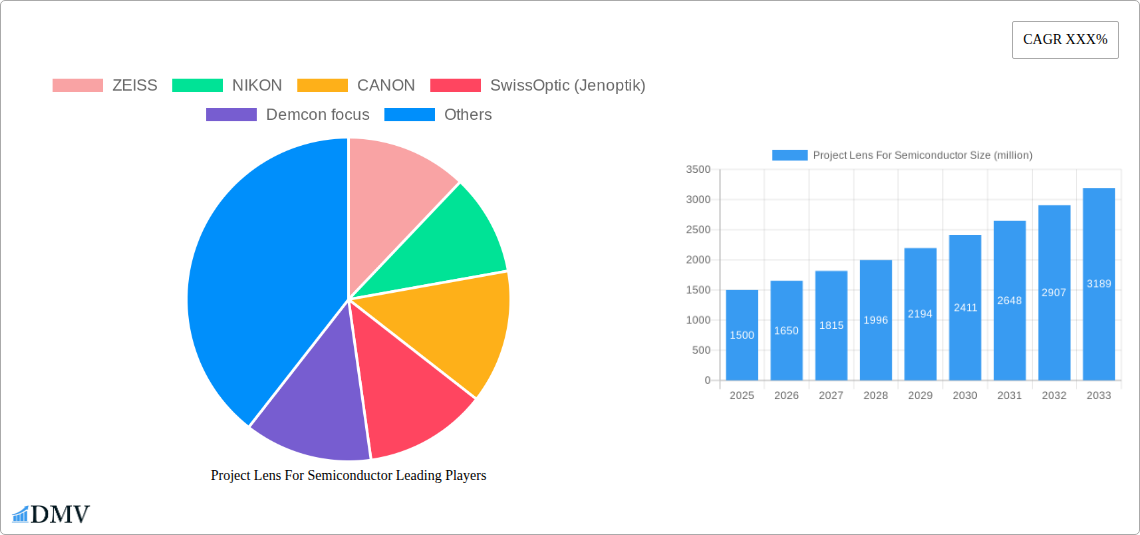
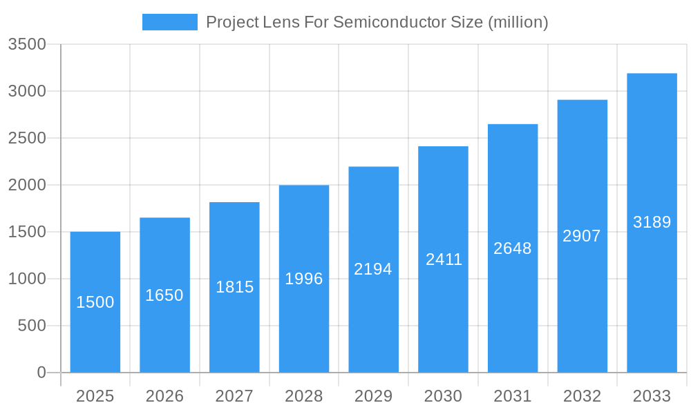
Project Lens For Semiconductor Market Size (In Billion)
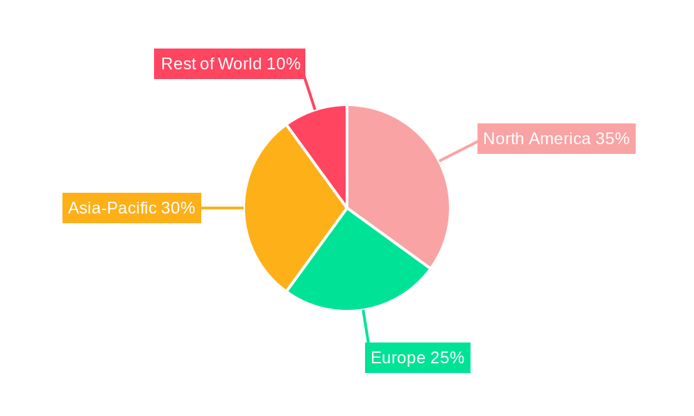
The forecast period from 2025 to 2033 anticipates a Compound Annual Growth Rate (CAGR) that reflects the continuing miniaturization trends in chip manufacturing and the increasing sophistication of semiconductor devices. Market segmentation is likely to be driven by lens type (e.g., UV, deep-UV, EUV), application (lithography, metrology, inspection), and end-user (foundries, memory manufacturers, etc.). Regional analysis will probably reveal strong growth in Asia-Pacific, primarily driven by the significant concentration of semiconductor manufacturing facilities in this region. North America and Europe will also maintain significant market share due to the presence of leading semiconductor companies and research institutions. Overall, the market is characterized by technological innovation, strategic partnerships, and a continuous drive towards improved imaging performance, which will be critical to the success of next-generation semiconductor production.
Project Lens For Semiconductor Company Market Share
Project Lens For Semiconductor Market Report: 2019-2033
This comprehensive report provides an in-depth analysis of the Project Lens For Semiconductor market, projecting a market value of $XX million by 2033. The study covers the historical period (2019-2024), the base year (2025), and the forecast period (2025-2033). It meticulously examines market dynamics, technological advancements, competitive landscapes, and future growth opportunities, offering invaluable insights for stakeholders across the semiconductor industry.
Project Lens For Semiconductor Market Composition & Trends
This section delves into the intricate structure of the Project Lens For Semiconductor market, evaluating its concentration, innovation drivers, regulatory environment, substitute products, end-user profiles, and merger & acquisition (M&A) activities. The market is characterized by a moderately concentrated landscape, with key players such as ZEISS, NIKON, and CANON holding significant market shares. However, emerging players like LIG Nanowise and Demcon focus are steadily increasing their presence through strategic innovations. The report quantifies market share distribution for each major player, providing a detailed competitive analysis and presenting data on M&A deal values exceeding $XX million in the past five years. Innovation is driven primarily by the increasing demand for higher resolution and precision in semiconductor manufacturing. Regulatory landscapes vary across regions, impacting market growth and investment strategies. The report explores the impact of substitutes, such as alternative inspection techniques, and profiles key end-users, encompassing leading semiconductor manufacturers and research institutions.
Project Lens For Semiconductor Industry Evolution
This section provides a detailed analysis of the Project Lens For Semiconductor market's evolution from 2019 to 2033. The market has witnessed a Compound Annual Growth Rate (CAGR) of XX% during the historical period (2019-2024), driven by advancements in lens technology, particularly in areas like high-NA lenses and advanced materials. Technological advancements like the integration of AI and machine learning in lens design and manufacturing are shaping the market's trajectory. The increasing complexity of semiconductor fabrication processes fuels the demand for higher-precision lenses, further boosting market growth. Consumer demand is shifting towards more efficient, reliable, and cost-effective solutions, pushing manufacturers to innovate and optimize their products. The report projects a CAGR of XX% for the forecast period (2025-2033), with a market value reaching $XX million by 2033. Adoption rates for advanced lens technologies are expected to increase significantly, driven by factors such as improved yield rates and reduced production costs in semiconductor manufacturing.
Leading Regions, Countries, or Segments in Project Lens For Semiconductor
The report identifies [Region/Country] as the dominant region/country in the Project Lens For Semiconductor market. This dominance is attributed to several factors:
- High Concentration of Semiconductor Manufacturers: A significant concentration of major semiconductor fabrication facilities drives the demand for high-quality lenses.
- Government Support and Investment: Generous government subsidies and investment in R&D enhance technological advancements and boost domestic manufacturing.
- Robust Infrastructure: A well-developed infrastructure facilitates efficient logistics and supply chain management.
- Favorable Regulatory Environment: Supportive regulatory policies reduce barriers to entry and encourage market growth.
This region's continued dominance is expected to propel overall market growth in the coming years. Detailed analyses of market dynamics within this leading region are incorporated, providing a nuanced understanding of the factors contributing to its success.
Project Lens For Semiconductor Product Innovations
Recent innovations in Project Lens For Semiconductor include the development of high-numerical aperture (NA) lenses, enabling higher resolution imaging for advanced node semiconductor manufacturing. The integration of novel materials like diffractive optics further enhances lens performance, improving image quality and reducing aberrations. These advancements translate to improved yield rates and reduced costs in semiconductor production, making them highly attractive to manufacturers. Unique selling propositions (USPs) include improved precision, enhanced durability, and optimized throughput.
Propelling Factors for Project Lens For Semiconductor Growth
The Project Lens For Semiconductor market is experiencing substantial growth propelled by several key factors. Technological advancements, such as the development of higher-NA lenses and advanced materials, continuously improve the performance and capabilities of these lenses. The increasing demand for smaller and more powerful semiconductor chips fuels the need for higher-precision lenses in fabrication processes. Furthermore, favorable government policies and investments in research and development stimulate innovation and market expansion.
Obstacles in the Project Lens For Semiconductor Market
Several challenges impede the growth of the Project Lens For Semiconductor market. Stringent regulatory requirements and compliance standards can increase production costs and hinder market penetration. Supply chain disruptions, particularly in the sourcing of specialized materials, can affect production timelines and lead to increased costs. Intense competition among established players and the emergence of new entrants create pressure on pricing and profitability. The overall impact of these factors leads to an estimated reduction in market growth of XX% in specific regions.
Future Opportunities in Project Lens For Semiconductor
Emerging opportunities in the Project Lens For Semiconductor market are abundant. The expansion into new applications, such as advanced packaging and 3D chip stacking, presents significant growth potential. The development of new materials and manufacturing techniques can further improve lens performance and cost-effectiveness. The growing demand for high-resolution imaging in other industries, such as life sciences and medical imaging, could open up new market segments.
Major Players in the Project Lens For Semiconductor Ecosystem
- ZEISS
- NIKON
- CANON
- SwissOptic (Jenoptik)
- Demcon focus
- LIG Nanowise
- Ushio
- In-Vision Technologies
- Sill Optics
- Photon Gear
Key Developments in Project Lens For Semiconductor Industry
- January 2023: ZEISS launched a new generation of high-NA lenses, significantly improving resolution capabilities.
- June 2022: NIKON announced a strategic partnership with a leading semiconductor manufacturer to develop customized lens solutions.
- October 2021: A major M&A deal involving two leading lens manufacturers resulted in a combined market share of XX%. Further details regarding deal values are included in the report's competitive landscape analysis.
Strategic Project Lens For Semiconductor Market Forecast
The Project Lens For Semiconductor market is poised for continued growth, driven by technological advancements, increasing demand from the semiconductor industry, and expanding applications in other sectors. The report's forecast indicates significant market expansion, driven by the rising adoption of advanced semiconductor manufacturing technologies. The development of innovative lens solutions and strategic partnerships among key players will further fuel growth, creating significant market opportunities for industry participants. The projected market value underscores the substantial potential of this sector.
Project Lens For Semiconductor Segmentation
-
1. Application
- 1.1. Wafer Factory
- 1.2. Integrated Device Manufacturer (IDMs)
-
2. Type
- 2.1. Below 200x
- 2.2. 200-240x
- 2.3. Above 240x
Project Lens For Semiconductor Segmentation By Geography
-
1. North America
- 1.1. United States
- 1.2. Canada
- 1.3. Mexico
-
2. South America
- 2.1. Brazil
- 2.2. Argentina
- 2.3. Rest of South America
-
3. Europe
- 3.1. United Kingdom
- 3.2. Germany
- 3.3. France
- 3.4. Italy
- 3.5. Spain
- 3.6. Russia
- 3.7. Benelux
- 3.8. Nordics
- 3.9. Rest of Europe
-
4. Middle East & Africa
- 4.1. Turkey
- 4.2. Israel
- 4.3. GCC
- 4.4. North Africa
- 4.5. South Africa
- 4.6. Rest of Middle East & Africa
-
5. Asia Pacific
- 5.1. China
- 5.2. India
- 5.3. Japan
- 5.4. South Korea
- 5.5. ASEAN
- 5.6. Oceania
- 5.7. Rest of Asia Pacific
Project Lens For Semiconductor Regional Market Share
Geographic Coverage of Project Lens For Semiconductor
Project Lens For Semiconductor REPORT HIGHLIGHTS
| Aspects | Details |
|---|---|
| Study Period | 2020-2034 |
| Base Year | 2025 |
| Estimated Year | 2026 |
| Forecast Period | 2026-2034 |
| Historical Period | 2020-2025 |
| Growth Rate | CAGR of XXX% from 2020-2034 |
| Segmentation |
|
Table of Contents
- 1. Introduction
- 1.1. Research Scope
- 1.2. Market Segmentation
- 1.3. Research Objective
- 1.4. Definitions and Assumptions
- 2. Executive Summary
- 2.1. Market Snapshot
- 3. Market Dynamics
- 3.1. Market Drivers
- 3.2. Market Restrains
- 3.3. Market Trends
- 3.4. Market Opportunities
- 4. Market Factor Analysis
- 4.1. Porters Five Forces
- 4.1.1. Bargaining Power of Suppliers
- 4.1.2. Bargaining Power of Buyers
- 4.1.3. Threat of New Entrants
- 4.1.4. Threat of Substitutes
- 4.1.5. Competitive Rivalry
- 4.2. PESTEL analysis
- 4.3. BCG Analysis
- 4.3.1. Stars (High Growth, High Market Share)
- 4.3.2. Cash Cows (Low Growth, High Market Share)
- 4.3.3. Question Mark (High Growth, Low Market Share)
- 4.3.4. Dogs (Low Growth, Low Market Share)
- 4.4. Ansoff Matrix Analysis
- 4.5. Supply Chain Analysis
- 4.6. Regulatory Landscape
- 4.7. Current Market Potential and Opportunity Assessment (TAM–SAM–SOM Framework)
- 4.8. DMV Analyst Note
- 4.1. Porters Five Forces
- 5. Market Analysis, Insights and Forecast 2021-2033
- 5.1. Market Analysis, Insights and Forecast - by Application
- 5.1.1. Wafer Factory
- 5.1.2. Integrated Device Manufacturer (IDMs)
- 5.2. Market Analysis, Insights and Forecast - by Type
- 5.2.1. Below 200x
- 5.2.2. 200-240x
- 5.2.3. Above 240x
- 5.3. Market Analysis, Insights and Forecast - by Region
- 5.3.1. North America
- 5.3.2. South America
- 5.3.3. Europe
- 5.3.4. Middle East & Africa
- 5.3.5. Asia Pacific
- 5.1. Market Analysis, Insights and Forecast - by Application
- 6. Global Project Lens For Semiconductor Analysis, Insights and Forecast, 2021-2033
- 6.1. Market Analysis, Insights and Forecast - by Application
- 6.1.1. Wafer Factory
- 6.1.2. Integrated Device Manufacturer (IDMs)
- 6.2. Market Analysis, Insights and Forecast - by Type
- 6.2.1. Below 200x
- 6.2.2. 200-240x
- 6.2.3. Above 240x
- 6.1. Market Analysis, Insights and Forecast - by Application
- 7. North America Project Lens For Semiconductor Analysis, Insights and Forecast, 2020-2032
- 7.1. Market Analysis, Insights and Forecast - by Application
- 7.1.1. Wafer Factory
- 7.1.2. Integrated Device Manufacturer (IDMs)
- 7.2. Market Analysis, Insights and Forecast - by Type
- 7.2.1. Below 200x
- 7.2.2. 200-240x
- 7.2.3. Above 240x
- 7.1. Market Analysis, Insights and Forecast - by Application
- 8. South America Project Lens For Semiconductor Analysis, Insights and Forecast, 2020-2032
- 8.1. Market Analysis, Insights and Forecast - by Application
- 8.1.1. Wafer Factory
- 8.1.2. Integrated Device Manufacturer (IDMs)
- 8.2. Market Analysis, Insights and Forecast - by Type
- 8.2.1. Below 200x
- 8.2.2. 200-240x
- 8.2.3. Above 240x
- 8.1. Market Analysis, Insights and Forecast - by Application
- 9. Europe Project Lens For Semiconductor Analysis, Insights and Forecast, 2020-2032
- 9.1. Market Analysis, Insights and Forecast - by Application
- 9.1.1. Wafer Factory
- 9.1.2. Integrated Device Manufacturer (IDMs)
- 9.2. Market Analysis, Insights and Forecast - by Type
- 9.2.1. Below 200x
- 9.2.2. 200-240x
- 9.2.3. Above 240x
- 9.1. Market Analysis, Insights and Forecast - by Application
- 10. Middle East & Africa Project Lens For Semiconductor Analysis, Insights and Forecast, 2020-2032
- 10.1. Market Analysis, Insights and Forecast - by Application
- 10.1.1. Wafer Factory
- 10.1.2. Integrated Device Manufacturer (IDMs)
- 10.2. Market Analysis, Insights and Forecast - by Type
- 10.2.1. Below 200x
- 10.2.2. 200-240x
- 10.2.3. Above 240x
- 10.1. Market Analysis, Insights and Forecast - by Application
- 11. Asia Pacific Project Lens For Semiconductor Analysis, Insights and Forecast, 2020-2032
- 11.1. Market Analysis, Insights and Forecast - by Application
- 11.1.1. Wafer Factory
- 11.1.2. Integrated Device Manufacturer (IDMs)
- 11.2. Market Analysis, Insights and Forecast - by Type
- 11.2.1. Below 200x
- 11.2.2. 200-240x
- 11.2.3. Above 240x
- 11.1. Market Analysis, Insights and Forecast - by Application
- 12. Competitive Analysis
- 12.1. Company Profiles
- 12.1.1 ZEISS
- 12.1.1.1. Company Overview
- 12.1.1.2. Products
- 12.1.1.3. Company Financials
- 12.1.1.4. SWOT Analysis
- 12.1.2 NIKON
- 12.1.2.1. Company Overview
- 12.1.2.2. Products
- 12.1.2.3. Company Financials
- 12.1.2.4. SWOT Analysis
- 12.1.3 CANON
- 12.1.3.1. Company Overview
- 12.1.3.2. Products
- 12.1.3.3. Company Financials
- 12.1.3.4. SWOT Analysis
- 12.1.4 SwissOptic (Jenoptik)
- 12.1.4.1. Company Overview
- 12.1.4.2. Products
- 12.1.4.3. Company Financials
- 12.1.4.4. SWOT Analysis
- 12.1.5 Demcon focus
- 12.1.5.1. Company Overview
- 12.1.5.2. Products
- 12.1.5.3. Company Financials
- 12.1.5.4. SWOT Analysis
- 12.1.6 LIG Nanowise
- 12.1.6.1. Company Overview
- 12.1.6.2. Products
- 12.1.6.3. Company Financials
- 12.1.6.4. SWOT Analysis
- 12.1.7 Ushio
- 12.1.7.1. Company Overview
- 12.1.7.2. Products
- 12.1.7.3. Company Financials
- 12.1.7.4. SWOT Analysis
- 12.1.8 In-Vision Technologies
- 12.1.8.1. Company Overview
- 12.1.8.2. Products
- 12.1.8.3. Company Financials
- 12.1.8.4. SWOT Analysis
- 12.1.9 Sill Optics
- 12.1.9.1. Company Overview
- 12.1.9.2. Products
- 12.1.9.3. Company Financials
- 12.1.9.4. SWOT Analysis
- 12.1.10 Photon Gear
- 12.1.10.1. Company Overview
- 12.1.10.2. Products
- 12.1.10.3. Company Financials
- 12.1.10.4. SWOT Analysis
- 12.1.1 ZEISS
- 12.2. Market Entropy
- 12.2.1 Company's Key Areas Served
- 12.2.2 Recent Developments
- 12.3. Company Market Share Analysis 2025
- 12.3.1 Top 5 Companies Market Share Analysis
- 12.3.2 Top 3 Companies Market Share Analysis
- 12.4. List of Potential Customers
- 13. Research Methodology
List of Figures
- Figure 1: Global Project Lens For Semiconductor Revenue Breakdown (million, %) by Region 2025 & 2033
- Figure 2: North America Project Lens For Semiconductor Revenue (million), by Application 2025 & 2033
- Figure 3: North America Project Lens For Semiconductor Revenue Share (%), by Application 2025 & 2033
- Figure 4: North America Project Lens For Semiconductor Revenue (million), by Type 2025 & 2033
- Figure 5: North America Project Lens For Semiconductor Revenue Share (%), by Type 2025 & 2033
- Figure 6: North America Project Lens For Semiconductor Revenue (million), by Country 2025 & 2033
- Figure 7: North America Project Lens For Semiconductor Revenue Share (%), by Country 2025 & 2033
- Figure 8: South America Project Lens For Semiconductor Revenue (million), by Application 2025 & 2033
- Figure 9: South America Project Lens For Semiconductor Revenue Share (%), by Application 2025 & 2033
- Figure 10: South America Project Lens For Semiconductor Revenue (million), by Type 2025 & 2033
- Figure 11: South America Project Lens For Semiconductor Revenue Share (%), by Type 2025 & 2033
- Figure 12: South America Project Lens For Semiconductor Revenue (million), by Country 2025 & 2033
- Figure 13: South America Project Lens For Semiconductor Revenue Share (%), by Country 2025 & 2033
- Figure 14: Europe Project Lens For Semiconductor Revenue (million), by Application 2025 & 2033
- Figure 15: Europe Project Lens For Semiconductor Revenue Share (%), by Application 2025 & 2033
- Figure 16: Europe Project Lens For Semiconductor Revenue (million), by Type 2025 & 2033
- Figure 17: Europe Project Lens For Semiconductor Revenue Share (%), by Type 2025 & 2033
- Figure 18: Europe Project Lens For Semiconductor Revenue (million), by Country 2025 & 2033
- Figure 19: Europe Project Lens For Semiconductor Revenue Share (%), by Country 2025 & 2033
- Figure 20: Middle East & Africa Project Lens For Semiconductor Revenue (million), by Application 2025 & 2033
- Figure 21: Middle East & Africa Project Lens For Semiconductor Revenue Share (%), by Application 2025 & 2033
- Figure 22: Middle East & Africa Project Lens For Semiconductor Revenue (million), by Type 2025 & 2033
- Figure 23: Middle East & Africa Project Lens For Semiconductor Revenue Share (%), by Type 2025 & 2033
- Figure 24: Middle East & Africa Project Lens For Semiconductor Revenue (million), by Country 2025 & 2033
- Figure 25: Middle East & Africa Project Lens For Semiconductor Revenue Share (%), by Country 2025 & 2033
- Figure 26: Asia Pacific Project Lens For Semiconductor Revenue (million), by Application 2025 & 2033
- Figure 27: Asia Pacific Project Lens For Semiconductor Revenue Share (%), by Application 2025 & 2033
- Figure 28: Asia Pacific Project Lens For Semiconductor Revenue (million), by Type 2025 & 2033
- Figure 29: Asia Pacific Project Lens For Semiconductor Revenue Share (%), by Type 2025 & 2033
- Figure 30: Asia Pacific Project Lens For Semiconductor Revenue (million), by Country 2025 & 2033
- Figure 31: Asia Pacific Project Lens For Semiconductor Revenue Share (%), by Country 2025 & 2033
List of Tables
- Table 1: Global Project Lens For Semiconductor Revenue million Forecast, by Application 2020 & 2033
- Table 2: Global Project Lens For Semiconductor Revenue million Forecast, by Type 2020 & 2033
- Table 3: Global Project Lens For Semiconductor Revenue million Forecast, by Region 2020 & 2033
- Table 4: Global Project Lens For Semiconductor Revenue million Forecast, by Application 2020 & 2033
- Table 5: Global Project Lens For Semiconductor Revenue million Forecast, by Type 2020 & 2033
- Table 6: Global Project Lens For Semiconductor Revenue million Forecast, by Country 2020 & 2033
- Table 7: United States Project Lens For Semiconductor Revenue (million) Forecast, by Application 2020 & 2033
- Table 8: Canada Project Lens For Semiconductor Revenue (million) Forecast, by Application 2020 & 2033
- Table 9: Mexico Project Lens For Semiconductor Revenue (million) Forecast, by Application 2020 & 2033
- Table 10: Global Project Lens For Semiconductor Revenue million Forecast, by Application 2020 & 2033
- Table 11: Global Project Lens For Semiconductor Revenue million Forecast, by Type 2020 & 2033
- Table 12: Global Project Lens For Semiconductor Revenue million Forecast, by Country 2020 & 2033
- Table 13: Brazil Project Lens For Semiconductor Revenue (million) Forecast, by Application 2020 & 2033
- Table 14: Argentina Project Lens For Semiconductor Revenue (million) Forecast, by Application 2020 & 2033
- Table 15: Rest of South America Project Lens For Semiconductor Revenue (million) Forecast, by Application 2020 & 2033
- Table 16: Global Project Lens For Semiconductor Revenue million Forecast, by Application 2020 & 2033
- Table 17: Global Project Lens For Semiconductor Revenue million Forecast, by Type 2020 & 2033
- Table 18: Global Project Lens For Semiconductor Revenue million Forecast, by Country 2020 & 2033
- Table 19: United Kingdom Project Lens For Semiconductor Revenue (million) Forecast, by Application 2020 & 2033
- Table 20: Germany Project Lens For Semiconductor Revenue (million) Forecast, by Application 2020 & 2033
- Table 21: France Project Lens For Semiconductor Revenue (million) Forecast, by Application 2020 & 2033
- Table 22: Italy Project Lens For Semiconductor Revenue (million) Forecast, by Application 2020 & 2033
- Table 23: Spain Project Lens For Semiconductor Revenue (million) Forecast, by Application 2020 & 2033
- Table 24: Russia Project Lens For Semiconductor Revenue (million) Forecast, by Application 2020 & 2033
- Table 25: Benelux Project Lens For Semiconductor Revenue (million) Forecast, by Application 2020 & 2033
- Table 26: Nordics Project Lens For Semiconductor Revenue (million) Forecast, by Application 2020 & 2033
- Table 27: Rest of Europe Project Lens For Semiconductor Revenue (million) Forecast, by Application 2020 & 2033
- Table 28: Global Project Lens For Semiconductor Revenue million Forecast, by Application 2020 & 2033
- Table 29: Global Project Lens For Semiconductor Revenue million Forecast, by Type 2020 & 2033
- Table 30: Global Project Lens For Semiconductor Revenue million Forecast, by Country 2020 & 2033
- Table 31: Turkey Project Lens For Semiconductor Revenue (million) Forecast, by Application 2020 & 2033
- Table 32: Israel Project Lens For Semiconductor Revenue (million) Forecast, by Application 2020 & 2033
- Table 33: GCC Project Lens For Semiconductor Revenue (million) Forecast, by Application 2020 & 2033
- Table 34: North Africa Project Lens For Semiconductor Revenue (million) Forecast, by Application 2020 & 2033
- Table 35: South Africa Project Lens For Semiconductor Revenue (million) Forecast, by Application 2020 & 2033
- Table 36: Rest of Middle East & Africa Project Lens For Semiconductor Revenue (million) Forecast, by Application 2020 & 2033
- Table 37: Global Project Lens For Semiconductor Revenue million Forecast, by Application 2020 & 2033
- Table 38: Global Project Lens For Semiconductor Revenue million Forecast, by Type 2020 & 2033
- Table 39: Global Project Lens For Semiconductor Revenue million Forecast, by Country 2020 & 2033
- Table 40: China Project Lens For Semiconductor Revenue (million) Forecast, by Application 2020 & 2033
- Table 41: India Project Lens For Semiconductor Revenue (million) Forecast, by Application 2020 & 2033
- Table 42: Japan Project Lens For Semiconductor Revenue (million) Forecast, by Application 2020 & 2033
- Table 43: South Korea Project Lens For Semiconductor Revenue (million) Forecast, by Application 2020 & 2033
- Table 44: ASEAN Project Lens For Semiconductor Revenue (million) Forecast, by Application 2020 & 2033
- Table 45: Oceania Project Lens For Semiconductor Revenue (million) Forecast, by Application 2020 & 2033
- Table 46: Rest of Asia Pacific Project Lens For Semiconductor Revenue (million) Forecast, by Application 2020 & 2033
Frequently Asked Questions
1. What is the projected Compound Annual Growth Rate (CAGR) of the Project Lens For Semiconductor?
The projected CAGR is approximately XXX%.
2. Which companies are prominent players in the Project Lens For Semiconductor?
Key companies in the market include ZEISS, NIKON, CANON, SwissOptic (Jenoptik), Demcon focus, LIG Nanowise, Ushio, In-Vision Technologies, Sill Optics, Photon Gear.
3. What are the main segments of the Project Lens For Semiconductor?
The market segments include Application, Type.
4. Can you provide details about the market size?
The market size is estimated to be USD XXX million as of 2022.
5. What are some drivers contributing to market growth?
N/A
6. What are the notable trends driving market growth?
N/A
7. Are there any restraints impacting market growth?
N/A
8. Can you provide examples of recent developments in the market?
N/A
9. What pricing options are available for accessing the report?
Pricing options include single-user, multi-user, and enterprise licenses priced at USD 2900.00, USD 4350.00, and USD 5800.00 respectively.
10. Is the market size provided in terms of value or volume?
The market size is provided in terms of value, measured in million.
11. Are there any specific market keywords associated with the report?
Yes, the market keyword associated with the report is "Project Lens For Semiconductor," which aids in identifying and referencing the specific market segment covered.
12. How do I determine which pricing option suits my needs best?
The pricing options vary based on user requirements and access needs. Individual users may opt for single-user licenses, while businesses requiring broader access may choose multi-user or enterprise licenses for cost-effective access to the report.
13. Are there any additional resources or data provided in the Project Lens For Semiconductor report?
While the report offers comprehensive insights, it's advisable to review the specific contents or supplementary materials provided to ascertain if additional resources or data are available.
14. How can I stay updated on further developments or reports in the Project Lens For Semiconductor?
To stay informed about further developments, trends, and reports in the Project Lens For Semiconductor, consider subscribing to industry newsletters, following relevant companies and organizations, or regularly checking reputable industry news sources and publications.
Methodology
Step 1 - Identification of Relevant Samples Size from Population Database


Step 2 - Approaches for Defining Global Market Size (Value, Volume* & Price*)

Note*: In applicable scenarios
Step 3 - Data Sources
Primary Research
- Web Analytics
- Survey Reports
- Research Institute
- Latest Research Reports
- Opinion Leaders
Secondary Research
- Annual Reports
- White Paper
- Latest Press Release
- Industry Association
- Paid Database
- Investor Presentations

Step 4 - Data Triangulation
Involves using different sources of information in order to increase the validity of a study
These sources are likely to be stakeholders in a program - participants, other researchers, program staff, other community members, and so on.
Then we put all data in single framework & apply various statistical tools to find out the dynamic on the market.
During the analysis stage, feedback from the stakeholder groups would be compared to determine areas of agreement as well as areas of divergence