

Key Insights
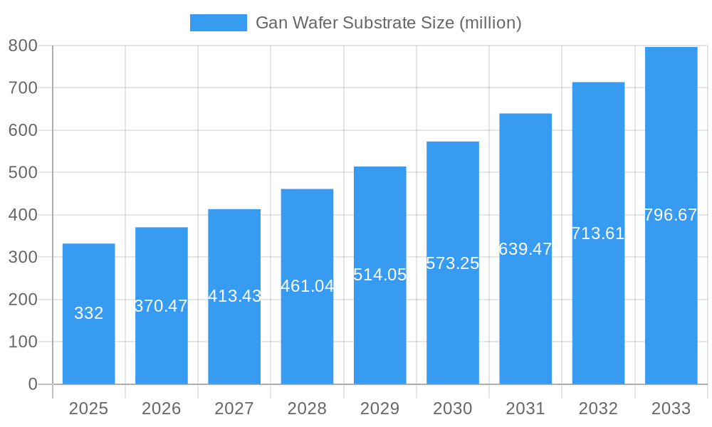
The Gallium Nitride (GaN) wafer substrate market is poised for significant expansion, projected to reach \$332 million and grow at an impressive Compound Annual Growth Rate (CAGR) of 11.6% from 2025 to 2033. This robust growth is primarily fueled by the escalating demand for high-performance electronic devices across various sectors. Key drivers include the widespread adoption of GaN technology in power electronic devices, such as efficient power supplies for consumer electronics, electric vehicles, and renewable energy systems. Furthermore, the increasing integration of GaN in high-frequency electronic devices for telecommunications, particularly with the rollout of 5G infrastructure, and in laser diodes for advanced lighting and sensing applications, is a substantial growth catalyst. The inherent advantages of GaN, including its high power density, superior thermal conductivity, and faster switching speeds compared to traditional silicon, make it an indispensable material for next-generation electronics.
Gan Wafer Substrate Market Size (In Million)
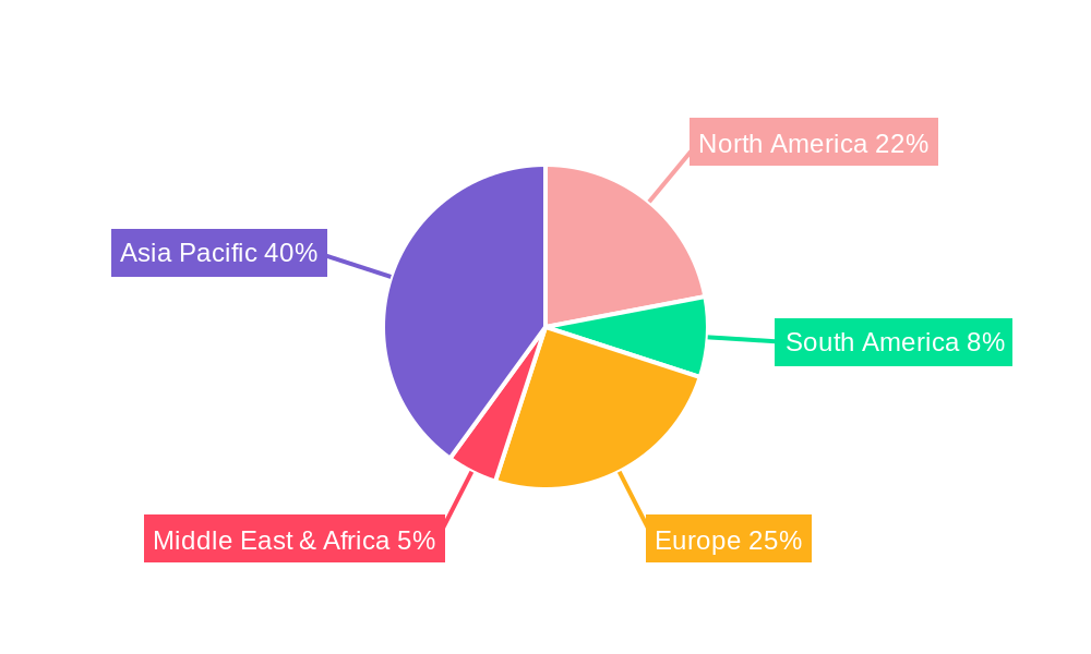
The market is characterized by a dynamic landscape of key players, including Sumitomo Electric Device Innovations (SEDI), Mitsubishi Chemical, Eta Research Ltd, Suzhou Nanowin Science and Technology, and Sanan Optoelectronics, among others, all vying for market share through innovation and strategic partnerships. The GaN wafer substrate market is segmented by application, with Laser Diodes, Power Electronic Devices, and High Frequency Electronic Devices emerging as the dominant segments, collectively driving the bulk of market demand. The "Others" segment, encompassing emerging applications, also presents promising growth potential. In terms of type, 2-inch and 4-inch GaN wafers are currently the most prevalent, catering to established manufacturing processes, while advancements in larger wafer sizes are anticipated to further optimize production costs and efficiency. Geographically, the Asia Pacific region, led by China, Japan, and South Korea, is expected to dominate the market due to its strong manufacturing base and rapid technological adoption, followed by North America and Europe, which are also witnessing substantial investment in GaN-based technologies.
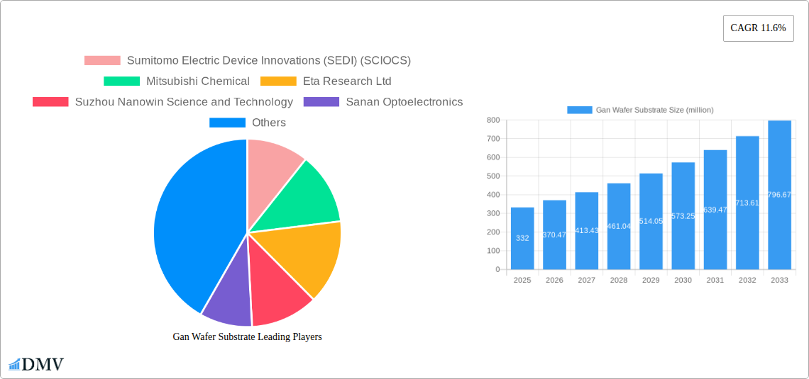
Gan Wafer Substrate Company Market Share
Gan Wafer Substrate Market Composition & Trends
The global Gan Wafer Substrate market is characterized by a dynamic interplay of established giants and emerging innovators, with market concentration evolving alongside technological advancements. Key players like Sumitomo Electric Device Innovations (SEDI) (SCIOCS) and Mitsubishi Chemical command significant market share, estimated to be over $500 million and $400 million respectively in the base year of 2025. However, agile companies such as Eta Research Ltd, Suzhou Nanowin Science and Technology, Sanan Optoelectronics, and Sino Nitride Semiconductor are rapidly gaining traction, driven by specialized innovations and cost-effective manufacturing. The market's innovation catalysts are primarily centered around improving wafer quality, reducing defect densities, and enhancing epitaxy processes for higher performance devices. Regulatory landscapes, particularly those focused on energy efficiency and advanced electronics manufacturing, are increasingly shaping market entry and expansion strategies. Substitute products, primarily silicon-based substrates, continue to pose a challenge, but the superior performance characteristics of GaN for high-frequency and high-power applications are widening the gap. End-user profiles are diverse, spanning consumer electronics, telecommunications, automotive, and defense sectors, with a growing demand from power electronics devices and high frequency electronic devices. Mergers and acquisitions (M&A) activities are expected to rise, with estimated deal values potentially reaching over $300 million in the forecast period, as larger players seek to consolidate their market position and acquire critical intellectual property. The distribution of market share is estimated to shift, with specialized GaN wafer segments projected to grow by 15% annually, while broader market growth is anticipated at a steady 12%.
- Market Share Distribution (Base Year 2025 - Estimated):
- Sumitomo Electric Device Innovations (SEDI) (SCIOCS): Approximately 25%
- Mitsubishi Chemical: Approximately 20%
- Other Major Players: Collectively 40%
- Emerging Players: Collectively 15%
- M&A Deal Value Trends:
- Historical M&A Value (2019-2024): Estimated to be over $200 million cumulatively.
- Forecasted M&A Value (2025-2033): Projected to exceed $300 million cumulatively, with individual significant deals potentially reaching over $100 million.
Gan Wafer Substrate Industry Evolution
The Gan Wafer Substrate industry has witnessed a remarkable evolution, transforming from a niche technology to a critical enabler of next-generation electronic devices. Throughout the historical period (2019–2024), the market experienced steady growth, driven by initial adoption in high-performance applications like RF power amplifiers and optoelectronics. During this phase, the market size grew from approximately $1.2 billion in 2019 to an estimated $2.5 billion by the end of 2024, reflecting a compound annual growth rate (CAGR) of around 15%. Technological advancements were paramount, focusing on improving crystal growth techniques, developing advanced epitaxy processes, and enhancing wafer defect reduction strategies. This period saw a significant push towards larger wafer diameters, with the emergence and increasing adoption of 4-inch GaN wafers, complementing the established 2-inch GaN wafer market.
As the market transitioned into the base year of 2025, estimated at $2.9 billion, the industry is poised for accelerated growth, with a projected CAGR of approximately 18% through the forecast period (2025–2033). This upswing is fueled by escalating demand from the power electronics sector, particularly for electric vehicles (EVs), renewable energy systems, and advanced power management solutions. The shift towards GaN-based power devices offers substantial advantages in terms of efficiency, size, and weight reduction compared to traditional silicon counterparts. Furthermore, the burgeoning 5G infrastructure and the increasing complexity of high-frequency electronic devices in telecommunications and radar systems are creating a robust demand for high-quality GaN wafers. Consumer adoption metrics for GaN-enabled devices, while still in their early stages, show a significant upward trend, with consumer electronics incorporating GaN components for faster charging and improved thermal management. The industry's commitment to innovation continues, with research and development efforts intensely focused on achieving defect-free wafers, cost reduction through scaled manufacturing, and the exploration of novel substrate materials and architectures. The increasing investment in GaN research and production facilities by major industry players underscores the industry's optimistic outlook and its pivotal role in the future of electronics.
Leading Regions, Countries, or Segments in Gan Wafer Substrate
The global Gan Wafer Substrate market exhibits distinct regional dominance and segment-specific growth patterns, with Asia Pacific emerging as the undisputed leader. Within this powerhouse region, China plays a pivotal role, driven by substantial government investment in advanced semiconductor manufacturing and a burgeoning domestic demand for high-performance electronic devices. The country's commitment to developing its indigenous semiconductor capabilities has led to significant expansions in GaN wafer production capacity, with companies like Suzhou Nanowin Science and Technology and Sanan Optoelectronics making substantial strides. Japan also remains a crucial hub, with established players like Sumitomo Electric Device Innovations (SEDI) (SCIOCS) and Mitsubishi Chemical continuing to drive innovation and maintain a strong market presence.
Among the applications, Power Electronic Devices are experiencing the most significant surge in demand, projected to account for over 40% of the total GaN wafer market by 2025, with an estimated market value of $1.2 billion. This growth is directly attributable to the relentless expansion of the electric vehicle industry, which requires highly efficient and compact power modules for inverters, converters, and onboard chargers. The renewable energy sector, including solar and wind power conversion systems, is another major contributor to the surge in demand for GaN power devices. The superior efficiency and high switching frequencies offered by GaN substrates enable smaller, lighter, and more energy-efficient power systems, aligning perfectly with global sustainability goals.
In terms of wafer type, 4-inch GaN Wafers are increasingly becoming the standard, projected to capture over 60% of the market share by 2025, with an estimated market value of $1.7 billion. This shift from 2-inch wafers is driven by the need for higher throughput in manufacturing and cost efficiencies associated with larger wafer sizes, which directly translates to reduced per-device costs for end-users. The development of advanced epitaxy technologies has enabled the consistent production of high-quality 4-inch GaN wafers, making them suitable for mass production of power and high-frequency devices.
- Dominant Region: Asia Pacific
- Key Country: China
- Drivers:
- Massive government investment in semiconductor self-sufficiency.
- Explosive domestic demand for EVs and 5G infrastructure.
- Significant R&D efforts and talent pool in semiconductor manufacturing.
- Growth of domestic GaN wafer manufacturers like Suzhou Nanowin and Sanan Optoelectronics.
- Drivers:
- Key Country: Japan
- Drivers:
- Long-standing expertise and innovation in materials science and semiconductor technology.
- Presence of established leaders like Sumitomo Electric Device Innovations (SEDI) (SCIOCS) and Mitsubishi Chemical.
- Strong focus on high-end applications and advanced R&D.
- Drivers:
- Key Country: China
- Dominant Application Segment: Power Electronic Devices
- Key Drivers:
- Electrification of transportation (EVs) requiring efficient and compact power solutions.
- Growth in renewable energy infrastructure and smart grids.
- Demand for energy-efficient consumer electronics and data centers.
- Improved performance metrics such as higher breakdown voltage and lower on-resistance compared to silicon.
- Key Drivers:
- Dominant Wafer Type: 4-inch GaN Wafer
- Key Drivers:
- Economies of scale in manufacturing leading to cost reductions.
- Increased throughput and productivity for device manufacturers.
- Technological advancements in epitaxy allowing for high-quality deposition on larger substrates.
- Alignment with industry standards for mass production of power and RF devices.
- Key Drivers:
Gan Wafer Substrate Product Innovations
Gan Wafer Substrate product innovations are sharply focused on enhancing device performance and reliability while reducing manufacturing costs. Manufacturers are achieving unprecedented levels of crystal quality, significantly lowering defect densities to less than 10^3 cm^-2, which is crucial for high-performance laser diodes and power electronics. Advancements in epitaxy techniques, such as Metal-Organic Chemical Vapor Deposition (MOCVD), allow for precise control over layer thickness and composition, enabling the creation of highly efficient transistors with lower on-resistance and faster switching speeds. Furthermore, innovations in buffer layers and substrate thinning are improving thermal management in power devices and enabling flexible GaN applications. These advancements translate to smaller, lighter, and more power-efficient devices for applications ranging from advanced lighting and sensing to high-speed data transmission.
Propelling Factors for Gan Wafer Substrate Growth
The explosive growth in the Gan Wafer Substrate market is propelled by a confluence of technological advancements, economic incentives, and supportive regulatory frameworks.
- Technological Superiority: GaN's inherent properties, including high electron mobility, wide bandgap, and high breakdown voltage, make it ideal for high-frequency, high-power, and high-temperature applications where silicon struggles. This translates to significantly more efficient and compact electronic devices.
- Expanding Application Spectrum: The adoption of GaN substrates is rapidly expanding beyond traditional RF applications into rapidly growing sectors like electric vehicles (EVs), renewable energy, 5G infrastructure, and advanced consumer electronics. The estimated market for GaN in EVs alone is projected to reach over $1 billion by 2028.
- Government Initiatives and Investments: Global governments are increasingly prioritizing the development of advanced semiconductor technologies. Significant investments in R&D, manufacturing subsidies, and favorable trade policies are accelerating the growth of the GaN wafer ecosystem, particularly in Asia.
- Cost-Effectiveness and Scalability: Continuous improvements in manufacturing processes, especially the transition to larger wafer diameters like 4-inch, are driving down production costs, making GaN-based devices more competitive and accessible. The projected reduction in wafer costs by 10% annually further bolsters this factor.
Obstacles in the Gan Wafer Substrate Market
Despite its promising trajectory, the Gan Wafer Substrate market faces several significant obstacles that could temper its growth.
- High Manufacturing Costs: While improving, the cost of producing high-quality GaN wafers remains higher than traditional silicon. This is due to complex manufacturing processes, specialized equipment, and the need for stringent quality control, with epitaxy costs still contributing significantly to the overall price.
- Supply Chain Bottlenecks and Material Availability: The specialized nature of GaN wafer manufacturing can lead to supply chain vulnerabilities. Shortages of critical raw materials or disruptions in the production of key components can impact overall output and lead times, with estimated lead times for some specialized materials extending to six months.
- Technical Challenges in Device Fabrication: While wafer quality is improving, challenges remain in device fabrication, including defect management and yield optimization for certain complex devices. Achieving near-zero defect densities across large wafer areas for all applications remains an ongoing R&D challenge.
- Limited Standardization and Interoperability: The lack of fully established industry standards for GaN wafer specifications and device interfaces can create interoperability issues for end-users and hinder wider market adoption.
Future Opportunities in Gan Wafer Substrate
The Gan Wafer Substrate market is ripe with emerging opportunities, driven by evolving technological demands and untapped application areas.
- Expansion into New Verticals: The superior performance of GaN presents significant opportunities in emerging sectors such as advanced medical devices, high-performance computing, and next-generation aerospace and defense systems.
- Development of Next-Generation GaN Devices: Continued innovation in device architectures, such as monolithic integration of power and RF functions, and the exploration of vertical GaN devices, promise even higher levels of performance and integration.
- Sustainable Energy Solutions: As the world transitions towards cleaner energy, the demand for highly efficient power conversion solutions for smart grids, electric aviation, and hydrogen fuel cells will significantly drive GaN wafer adoption.
- Miniaturization and IoT Growth: The drive for smaller, more power-efficient electronic components for the Internet of Things (IoT) and wearable devices opens up a vast market for micro-GaN devices.
Major Players in the Gan Wafer Substrate Ecosystem
- Sumitomo Electric Device Innovations (SEDI) (SCIOCS)
- Mitsubishi Chemical
- Eta Research Ltd
- Suzhou Nanowin Science and Technology
- Sanan Optoelectronics
- Sino Nitride Semiconductor
- Goetsu Semiconductor Wuxi
- BTOZ
- Toyoda Gosei
- Kyma Technologies
Key Developments in Gan Wafer Substrate Industry
- 2019: Sumitomo Electric Device Innovations (SEDI) (SCIOCS) announces a breakthrough in reducing defect density in 6-inch GaN-on-SiC wafers, paving the way for higher power RF applications.
- 2020: Mitsubishi Chemical launches a new high-performance GaN wafer substrate with improved thermal conductivity, enhancing thermal management capabilities for power devices.
- 2021: Sanan Optoelectronics secures significant funding for expanding its GaN wafer manufacturing capacity to meet the growing demand from the power electronics sector, with an investment exceeding $500 million.
- 2022: Eta Research Ltd develops a novel GaN epitaxy process that reduces growth time by 20%, leading to improved cost-efficiency for GaN wafer production.
- 2023: Suzhou Nanowin Science and Technology partners with a leading automotive manufacturer to develop GaN power modules for electric vehicle inverters, signaling strong industry adoption.
- 2024 (Q1): Sino Nitride Semiconductor announces the successful development of a 4-inch GaN-on-sapphire wafer with industry-leading uniformity, catering to high-frequency electronic device applications.
- 2024 (Q3): Goetsu Semiconductor Wuxi showcases advancements in large-diameter GaN wafer technology, demonstrating their commitment to scaling production for broader market accessibility.
- 2025 (Projected): A significant merger or acquisition is anticipated as larger players seek to consolidate market share and acquire key intellectual property in the rapidly evolving GaN substrate landscape.
Strategic Gan Wafer Substrate Market Forecast
The strategic outlook for the Gan Wafer Substrate market is exceptionally robust, driven by an increasing demand for high-performance, energy-efficient electronic solutions across multiple industries. The continued innovation in epitaxy and wafer processing, coupled with the expanding application base in power electronics and high-frequency devices, will be key growth catalysts. Investments in scaling production capacity and technological advancements aimed at cost reduction will further solidify GaN's competitive edge against silicon. Emerging markets and the growing need for advanced semiconductor technologies in defense and telecommunications present significant untapped potential, suggesting a future where GaN wafers are indispensable components of next-generation electronics. The market is projected to witness a sustained CAGR of over 15% through 2033, with a total market size anticipated to exceed $10 billion.
Gan Wafer Substrate Segmentation
-
1. Application
- 1.1. Laser Diodes
- 1.2. Power Electronic Devices
- 1.3. High Frequency Electronic Devices
- 1.4. Others
-
2. Type
- 2.1. 2 inch GaN Wafer
- 2.2. 4 inch GaN Wafer
- 2.3. Others
Gan Wafer Substrate Segmentation By Geography
-
1. North America
- 1.1. United States
- 1.2. Canada
- 1.3. Mexico
-
2. South America
- 2.1. Brazil
- 2.2. Argentina
- 2.3. Rest of South America
-
3. Europe
- 3.1. United Kingdom
- 3.2. Germany
- 3.3. France
- 3.4. Italy
- 3.5. Spain
- 3.6. Russia
- 3.7. Benelux
- 3.8. Nordics
- 3.9. Rest of Europe
-
4. Middle East & Africa
- 4.1. Turkey
- 4.2. Israel
- 4.3. GCC
- 4.4. North Africa
- 4.5. South Africa
- 4.6. Rest of Middle East & Africa
-
5. Asia Pacific
- 5.1. China
- 5.2. India
- 5.3. Japan
- 5.4. South Korea
- 5.5. ASEAN
- 5.6. Oceania
- 5.7. Rest of Asia Pacific
Gan Wafer Substrate Regional Market Share
Geographic Coverage of Gan Wafer Substrate
Gan Wafer Substrate REPORT HIGHLIGHTS
| Aspects | Details |
|---|---|
| Study Period | 2020-2034 |
| Base Year | 2025 |
| Estimated Year | 2026 |
| Forecast Period | 2026-2034 |
| Historical Period | 2020-2025 |
| Growth Rate | CAGR of 11.6% from 2020-2034 |
| Segmentation |
|
Table of Contents
- 1. Introduction
- 1.1. Research Scope
- 1.2. Market Segmentation
- 1.3. Research Objective
- 1.4. Definitions and Assumptions
- 2. Executive Summary
- 2.1. Market Snapshot
- 3. Market Dynamics
- 3.1. Market Drivers
- 3.2. Market Restrains
- 3.3. Market Trends
- 3.4. Market Opportunities
- 4. Market Factor Analysis
- 4.1. Porters Five Forces
- 4.1.1. Bargaining Power of Suppliers
- 4.1.2. Bargaining Power of Buyers
- 4.1.3. Threat of New Entrants
- 4.1.4. Threat of Substitutes
- 4.1.5. Competitive Rivalry
- 4.2. PESTEL analysis
- 4.3. BCG Analysis
- 4.3.1. Stars (High Growth, High Market Share)
- 4.3.2. Cash Cows (Low Growth, High Market Share)
- 4.3.3. Question Mark (High Growth, Low Market Share)
- 4.3.4. Dogs (Low Growth, Low Market Share)
- 4.4. Ansoff Matrix Analysis
- 4.5. Supply Chain Analysis
- 4.6. Regulatory Landscape
- 4.7. Current Market Potential and Opportunity Assessment (TAM–SAM–SOM Framework)
- 4.8. DMV Analyst Note
- 4.1. Porters Five Forces
- 5. Market Analysis, Insights and Forecast 2021-2033
- 5.1. Market Analysis, Insights and Forecast - by Application
- 5.1.1. Laser Diodes
- 5.1.2. Power Electronic Devices
- 5.1.3. High Frequency Electronic Devices
- 5.1.4. Others
- 5.2. Market Analysis, Insights and Forecast - by Type
- 5.2.1. 2 inch GaN Wafer
- 5.2.2. 4 inch GaN Wafer
- 5.2.3. Others
- 5.3. Market Analysis, Insights and Forecast - by Region
- 5.3.1. North America
- 5.3.2. South America
- 5.3.3. Europe
- 5.3.4. Middle East & Africa
- 5.3.5. Asia Pacific
- 5.1. Market Analysis, Insights and Forecast - by Application
- 6. Global Gan Wafer Substrate Analysis, Insights and Forecast, 2021-2033
- 6.1. Market Analysis, Insights and Forecast - by Application
- 6.1.1. Laser Diodes
- 6.1.2. Power Electronic Devices
- 6.1.3. High Frequency Electronic Devices
- 6.1.4. Others
- 6.2. Market Analysis, Insights and Forecast - by Type
- 6.2.1. 2 inch GaN Wafer
- 6.2.2. 4 inch GaN Wafer
- 6.2.3. Others
- 6.1. Market Analysis, Insights and Forecast - by Application
- 7. North America Gan Wafer Substrate Analysis, Insights and Forecast, 2020-2032
- 7.1. Market Analysis, Insights and Forecast - by Application
- 7.1.1. Laser Diodes
- 7.1.2. Power Electronic Devices
- 7.1.3. High Frequency Electronic Devices
- 7.1.4. Others
- 7.2. Market Analysis, Insights and Forecast - by Type
- 7.2.1. 2 inch GaN Wafer
- 7.2.2. 4 inch GaN Wafer
- 7.2.3. Others
- 7.1. Market Analysis, Insights and Forecast - by Application
- 8. South America Gan Wafer Substrate Analysis, Insights and Forecast, 2020-2032
- 8.1. Market Analysis, Insights and Forecast - by Application
- 8.1.1. Laser Diodes
- 8.1.2. Power Electronic Devices
- 8.1.3. High Frequency Electronic Devices
- 8.1.4. Others
- 8.2. Market Analysis, Insights and Forecast - by Type
- 8.2.1. 2 inch GaN Wafer
- 8.2.2. 4 inch GaN Wafer
- 8.2.3. Others
- 8.1. Market Analysis, Insights and Forecast - by Application
- 9. Europe Gan Wafer Substrate Analysis, Insights and Forecast, 2020-2032
- 9.1. Market Analysis, Insights and Forecast - by Application
- 9.1.1. Laser Diodes
- 9.1.2. Power Electronic Devices
- 9.1.3. High Frequency Electronic Devices
- 9.1.4. Others
- 9.2. Market Analysis, Insights and Forecast - by Type
- 9.2.1. 2 inch GaN Wafer
- 9.2.2. 4 inch GaN Wafer
- 9.2.3. Others
- 9.1. Market Analysis, Insights and Forecast - by Application
- 10. Middle East & Africa Gan Wafer Substrate Analysis, Insights and Forecast, 2020-2032
- 10.1. Market Analysis, Insights and Forecast - by Application
- 10.1.1. Laser Diodes
- 10.1.2. Power Electronic Devices
- 10.1.3. High Frequency Electronic Devices
- 10.1.4. Others
- 10.2. Market Analysis, Insights and Forecast - by Type
- 10.2.1. 2 inch GaN Wafer
- 10.2.2. 4 inch GaN Wafer
- 10.2.3. Others
- 10.1. Market Analysis, Insights and Forecast - by Application
- 11. Asia Pacific Gan Wafer Substrate Analysis, Insights and Forecast, 2020-2032
- 11.1. Market Analysis, Insights and Forecast - by Application
- 11.1.1. Laser Diodes
- 11.1.2. Power Electronic Devices
- 11.1.3. High Frequency Electronic Devices
- 11.1.4. Others
- 11.2. Market Analysis, Insights and Forecast - by Type
- 11.2.1. 2 inch GaN Wafer
- 11.2.2. 4 inch GaN Wafer
- 11.2.3. Others
- 11.1. Market Analysis, Insights and Forecast - by Application
- 12. Competitive Analysis
- 12.1. Company Profiles
- 12.1.1 Sumitomo Electric Device Innovations (SEDI) (SCIOCS)
- 12.1.1.1. Company Overview
- 12.1.1.2. Products
- 12.1.1.3. Company Financials
- 12.1.1.4. SWOT Analysis
- 12.1.2 Mitsubishi Chemical
- 12.1.2.1. Company Overview
- 12.1.2.2. Products
- 12.1.2.3. Company Financials
- 12.1.2.4. SWOT Analysis
- 12.1.3 Eta Research Ltd
- 12.1.3.1. Company Overview
- 12.1.3.2. Products
- 12.1.3.3. Company Financials
- 12.1.3.4. SWOT Analysis
- 12.1.4 Suzhou Nanowin Science and Technology
- 12.1.4.1. Company Overview
- 12.1.4.2. Products
- 12.1.4.3. Company Financials
- 12.1.4.4. SWOT Analysis
- 12.1.5 Sanan Optoelectronics
- 12.1.5.1. Company Overview
- 12.1.5.2. Products
- 12.1.5.3. Company Financials
- 12.1.5.4. SWOT Analysis
- 12.1.6 Sino Nitride Semiconductor
- 12.1.6.1. Company Overview
- 12.1.6.2. Products
- 12.1.6.3. Company Financials
- 12.1.6.4. SWOT Analysis
- 12.1.7 Goetsu Semiconductor Wuxi
- 12.1.7.1. Company Overview
- 12.1.7.2. Products
- 12.1.7.3. Company Financials
- 12.1.7.4. SWOT Analysis
- 12.1.8 BTOZ
- 12.1.8.1. Company Overview
- 12.1.8.2. Products
- 12.1.8.3. Company Financials
- 12.1.8.4. SWOT Analysis
- 12.1.9 Toyoda Gosei
- 12.1.9.1. Company Overview
- 12.1.9.2. Products
- 12.1.9.3. Company Financials
- 12.1.9.4. SWOT Analysis
- 12.1.10 Kyma Technologies
- 12.1.10.1. Company Overview
- 12.1.10.2. Products
- 12.1.10.3. Company Financials
- 12.1.10.4. SWOT Analysis
- 12.1.1 Sumitomo Electric Device Innovations (SEDI) (SCIOCS)
- 12.2. Market Entropy
- 12.2.1 Company's Key Areas Served
- 12.2.2 Recent Developments
- 12.3. Company Market Share Analysis 2025
- 12.3.1 Top 5 Companies Market Share Analysis
- 12.3.2 Top 3 Companies Market Share Analysis
- 12.4. List of Potential Customers
- 13. Research Methodology
List of Figures
- Figure 1: Global Gan Wafer Substrate Revenue Breakdown (million, %) by Region 2025 & 2033
- Figure 2: Global Gan Wafer Substrate Volume Breakdown (K, %) by Region 2025 & 2033
- Figure 3: North America Gan Wafer Substrate Revenue (million), by Application 2025 & 2033
- Figure 4: North America Gan Wafer Substrate Volume (K), by Application 2025 & 2033
- Figure 5: North America Gan Wafer Substrate Revenue Share (%), by Application 2025 & 2033
- Figure 6: North America Gan Wafer Substrate Volume Share (%), by Application 2025 & 2033
- Figure 7: North America Gan Wafer Substrate Revenue (million), by Type 2025 & 2033
- Figure 8: North America Gan Wafer Substrate Volume (K), by Type 2025 & 2033
- Figure 9: North America Gan Wafer Substrate Revenue Share (%), by Type 2025 & 2033
- Figure 10: North America Gan Wafer Substrate Volume Share (%), by Type 2025 & 2033
- Figure 11: North America Gan Wafer Substrate Revenue (million), by Country 2025 & 2033
- Figure 12: North America Gan Wafer Substrate Volume (K), by Country 2025 & 2033
- Figure 13: North America Gan Wafer Substrate Revenue Share (%), by Country 2025 & 2033
- Figure 14: North America Gan Wafer Substrate Volume Share (%), by Country 2025 & 2033
- Figure 15: South America Gan Wafer Substrate Revenue (million), by Application 2025 & 2033
- Figure 16: South America Gan Wafer Substrate Volume (K), by Application 2025 & 2033
- Figure 17: South America Gan Wafer Substrate Revenue Share (%), by Application 2025 & 2033
- Figure 18: South America Gan Wafer Substrate Volume Share (%), by Application 2025 & 2033
- Figure 19: South America Gan Wafer Substrate Revenue (million), by Type 2025 & 2033
- Figure 20: South America Gan Wafer Substrate Volume (K), by Type 2025 & 2033
- Figure 21: South America Gan Wafer Substrate Revenue Share (%), by Type 2025 & 2033
- Figure 22: South America Gan Wafer Substrate Volume Share (%), by Type 2025 & 2033
- Figure 23: South America Gan Wafer Substrate Revenue (million), by Country 2025 & 2033
- Figure 24: South America Gan Wafer Substrate Volume (K), by Country 2025 & 2033
- Figure 25: South America Gan Wafer Substrate Revenue Share (%), by Country 2025 & 2033
- Figure 26: South America Gan Wafer Substrate Volume Share (%), by Country 2025 & 2033
- Figure 27: Europe Gan Wafer Substrate Revenue (million), by Application 2025 & 2033
- Figure 28: Europe Gan Wafer Substrate Volume (K), by Application 2025 & 2033
- Figure 29: Europe Gan Wafer Substrate Revenue Share (%), by Application 2025 & 2033
- Figure 30: Europe Gan Wafer Substrate Volume Share (%), by Application 2025 & 2033
- Figure 31: Europe Gan Wafer Substrate Revenue (million), by Type 2025 & 2033
- Figure 32: Europe Gan Wafer Substrate Volume (K), by Type 2025 & 2033
- Figure 33: Europe Gan Wafer Substrate Revenue Share (%), by Type 2025 & 2033
- Figure 34: Europe Gan Wafer Substrate Volume Share (%), by Type 2025 & 2033
- Figure 35: Europe Gan Wafer Substrate Revenue (million), by Country 2025 & 2033
- Figure 36: Europe Gan Wafer Substrate Volume (K), by Country 2025 & 2033
- Figure 37: Europe Gan Wafer Substrate Revenue Share (%), by Country 2025 & 2033
- Figure 38: Europe Gan Wafer Substrate Volume Share (%), by Country 2025 & 2033
- Figure 39: Middle East & Africa Gan Wafer Substrate Revenue (million), by Application 2025 & 2033
- Figure 40: Middle East & Africa Gan Wafer Substrate Volume (K), by Application 2025 & 2033
- Figure 41: Middle East & Africa Gan Wafer Substrate Revenue Share (%), by Application 2025 & 2033
- Figure 42: Middle East & Africa Gan Wafer Substrate Volume Share (%), by Application 2025 & 2033
- Figure 43: Middle East & Africa Gan Wafer Substrate Revenue (million), by Type 2025 & 2033
- Figure 44: Middle East & Africa Gan Wafer Substrate Volume (K), by Type 2025 & 2033
- Figure 45: Middle East & Africa Gan Wafer Substrate Revenue Share (%), by Type 2025 & 2033
- Figure 46: Middle East & Africa Gan Wafer Substrate Volume Share (%), by Type 2025 & 2033
- Figure 47: Middle East & Africa Gan Wafer Substrate Revenue (million), by Country 2025 & 2033
- Figure 48: Middle East & Africa Gan Wafer Substrate Volume (K), by Country 2025 & 2033
- Figure 49: Middle East & Africa Gan Wafer Substrate Revenue Share (%), by Country 2025 & 2033
- Figure 50: Middle East & Africa Gan Wafer Substrate Volume Share (%), by Country 2025 & 2033
- Figure 51: Asia Pacific Gan Wafer Substrate Revenue (million), by Application 2025 & 2033
- Figure 52: Asia Pacific Gan Wafer Substrate Volume (K), by Application 2025 & 2033
- Figure 53: Asia Pacific Gan Wafer Substrate Revenue Share (%), by Application 2025 & 2033
- Figure 54: Asia Pacific Gan Wafer Substrate Volume Share (%), by Application 2025 & 2033
- Figure 55: Asia Pacific Gan Wafer Substrate Revenue (million), by Type 2025 & 2033
- Figure 56: Asia Pacific Gan Wafer Substrate Volume (K), by Type 2025 & 2033
- Figure 57: Asia Pacific Gan Wafer Substrate Revenue Share (%), by Type 2025 & 2033
- Figure 58: Asia Pacific Gan Wafer Substrate Volume Share (%), by Type 2025 & 2033
- Figure 59: Asia Pacific Gan Wafer Substrate Revenue (million), by Country 2025 & 2033
- Figure 60: Asia Pacific Gan Wafer Substrate Volume (K), by Country 2025 & 2033
- Figure 61: Asia Pacific Gan Wafer Substrate Revenue Share (%), by Country 2025 & 2033
- Figure 62: Asia Pacific Gan Wafer Substrate Volume Share (%), by Country 2025 & 2033
List of Tables
- Table 1: Global Gan Wafer Substrate Revenue million Forecast, by Application 2020 & 2033
- Table 2: Global Gan Wafer Substrate Volume K Forecast, by Application 2020 & 2033
- Table 3: Global Gan Wafer Substrate Revenue million Forecast, by Type 2020 & 2033
- Table 4: Global Gan Wafer Substrate Volume K Forecast, by Type 2020 & 2033
- Table 5: Global Gan Wafer Substrate Revenue million Forecast, by Region 2020 & 2033
- Table 6: Global Gan Wafer Substrate Volume K Forecast, by Region 2020 & 2033
- Table 7: Global Gan Wafer Substrate Revenue million Forecast, by Application 2020 & 2033
- Table 8: Global Gan Wafer Substrate Volume K Forecast, by Application 2020 & 2033
- Table 9: Global Gan Wafer Substrate Revenue million Forecast, by Type 2020 & 2033
- Table 10: Global Gan Wafer Substrate Volume K Forecast, by Type 2020 & 2033
- Table 11: Global Gan Wafer Substrate Revenue million Forecast, by Country 2020 & 2033
- Table 12: Global Gan Wafer Substrate Volume K Forecast, by Country 2020 & 2033
- Table 13: United States Gan Wafer Substrate Revenue (million) Forecast, by Application 2020 & 2033
- Table 14: United States Gan Wafer Substrate Volume (K) Forecast, by Application 2020 & 2033
- Table 15: Canada Gan Wafer Substrate Revenue (million) Forecast, by Application 2020 & 2033
- Table 16: Canada Gan Wafer Substrate Volume (K) Forecast, by Application 2020 & 2033
- Table 17: Mexico Gan Wafer Substrate Revenue (million) Forecast, by Application 2020 & 2033
- Table 18: Mexico Gan Wafer Substrate Volume (K) Forecast, by Application 2020 & 2033
- Table 19: Global Gan Wafer Substrate Revenue million Forecast, by Application 2020 & 2033
- Table 20: Global Gan Wafer Substrate Volume K Forecast, by Application 2020 & 2033
- Table 21: Global Gan Wafer Substrate Revenue million Forecast, by Type 2020 & 2033
- Table 22: Global Gan Wafer Substrate Volume K Forecast, by Type 2020 & 2033
- Table 23: Global Gan Wafer Substrate Revenue million Forecast, by Country 2020 & 2033
- Table 24: Global Gan Wafer Substrate Volume K Forecast, by Country 2020 & 2033
- Table 25: Brazil Gan Wafer Substrate Revenue (million) Forecast, by Application 2020 & 2033
- Table 26: Brazil Gan Wafer Substrate Volume (K) Forecast, by Application 2020 & 2033
- Table 27: Argentina Gan Wafer Substrate Revenue (million) Forecast, by Application 2020 & 2033
- Table 28: Argentina Gan Wafer Substrate Volume (K) Forecast, by Application 2020 & 2033
- Table 29: Rest of South America Gan Wafer Substrate Revenue (million) Forecast, by Application 2020 & 2033
- Table 30: Rest of South America Gan Wafer Substrate Volume (K) Forecast, by Application 2020 & 2033
- Table 31: Global Gan Wafer Substrate Revenue million Forecast, by Application 2020 & 2033
- Table 32: Global Gan Wafer Substrate Volume K Forecast, by Application 2020 & 2033
- Table 33: Global Gan Wafer Substrate Revenue million Forecast, by Type 2020 & 2033
- Table 34: Global Gan Wafer Substrate Volume K Forecast, by Type 2020 & 2033
- Table 35: Global Gan Wafer Substrate Revenue million Forecast, by Country 2020 & 2033
- Table 36: Global Gan Wafer Substrate Volume K Forecast, by Country 2020 & 2033
- Table 37: United Kingdom Gan Wafer Substrate Revenue (million) Forecast, by Application 2020 & 2033
- Table 38: United Kingdom Gan Wafer Substrate Volume (K) Forecast, by Application 2020 & 2033
- Table 39: Germany Gan Wafer Substrate Revenue (million) Forecast, by Application 2020 & 2033
- Table 40: Germany Gan Wafer Substrate Volume (K) Forecast, by Application 2020 & 2033
- Table 41: France Gan Wafer Substrate Revenue (million) Forecast, by Application 2020 & 2033
- Table 42: France Gan Wafer Substrate Volume (K) Forecast, by Application 2020 & 2033
- Table 43: Italy Gan Wafer Substrate Revenue (million) Forecast, by Application 2020 & 2033
- Table 44: Italy Gan Wafer Substrate Volume (K) Forecast, by Application 2020 & 2033
- Table 45: Spain Gan Wafer Substrate Revenue (million) Forecast, by Application 2020 & 2033
- Table 46: Spain Gan Wafer Substrate Volume (K) Forecast, by Application 2020 & 2033
- Table 47: Russia Gan Wafer Substrate Revenue (million) Forecast, by Application 2020 & 2033
- Table 48: Russia Gan Wafer Substrate Volume (K) Forecast, by Application 2020 & 2033
- Table 49: Benelux Gan Wafer Substrate Revenue (million) Forecast, by Application 2020 & 2033
- Table 50: Benelux Gan Wafer Substrate Volume (K) Forecast, by Application 2020 & 2033
- Table 51: Nordics Gan Wafer Substrate Revenue (million) Forecast, by Application 2020 & 2033
- Table 52: Nordics Gan Wafer Substrate Volume (K) Forecast, by Application 2020 & 2033
- Table 53: Rest of Europe Gan Wafer Substrate Revenue (million) Forecast, by Application 2020 & 2033
- Table 54: Rest of Europe Gan Wafer Substrate Volume (K) Forecast, by Application 2020 & 2033
- Table 55: Global Gan Wafer Substrate Revenue million Forecast, by Application 2020 & 2033
- Table 56: Global Gan Wafer Substrate Volume K Forecast, by Application 2020 & 2033
- Table 57: Global Gan Wafer Substrate Revenue million Forecast, by Type 2020 & 2033
- Table 58: Global Gan Wafer Substrate Volume K Forecast, by Type 2020 & 2033
- Table 59: Global Gan Wafer Substrate Revenue million Forecast, by Country 2020 & 2033
- Table 60: Global Gan Wafer Substrate Volume K Forecast, by Country 2020 & 2033
- Table 61: Turkey Gan Wafer Substrate Revenue (million) Forecast, by Application 2020 & 2033
- Table 62: Turkey Gan Wafer Substrate Volume (K) Forecast, by Application 2020 & 2033
- Table 63: Israel Gan Wafer Substrate Revenue (million) Forecast, by Application 2020 & 2033
- Table 64: Israel Gan Wafer Substrate Volume (K) Forecast, by Application 2020 & 2033
- Table 65: GCC Gan Wafer Substrate Revenue (million) Forecast, by Application 2020 & 2033
- Table 66: GCC Gan Wafer Substrate Volume (K) Forecast, by Application 2020 & 2033
- Table 67: North Africa Gan Wafer Substrate Revenue (million) Forecast, by Application 2020 & 2033
- Table 68: North Africa Gan Wafer Substrate Volume (K) Forecast, by Application 2020 & 2033
- Table 69: South Africa Gan Wafer Substrate Revenue (million) Forecast, by Application 2020 & 2033
- Table 70: South Africa Gan Wafer Substrate Volume (K) Forecast, by Application 2020 & 2033
- Table 71: Rest of Middle East & Africa Gan Wafer Substrate Revenue (million) Forecast, by Application 2020 & 2033
- Table 72: Rest of Middle East & Africa Gan Wafer Substrate Volume (K) Forecast, by Application 2020 & 2033
- Table 73: Global Gan Wafer Substrate Revenue million Forecast, by Application 2020 & 2033
- Table 74: Global Gan Wafer Substrate Volume K Forecast, by Application 2020 & 2033
- Table 75: Global Gan Wafer Substrate Revenue million Forecast, by Type 2020 & 2033
- Table 76: Global Gan Wafer Substrate Volume K Forecast, by Type 2020 & 2033
- Table 77: Global Gan Wafer Substrate Revenue million Forecast, by Country 2020 & 2033
- Table 78: Global Gan Wafer Substrate Volume K Forecast, by Country 2020 & 2033
- Table 79: China Gan Wafer Substrate Revenue (million) Forecast, by Application 2020 & 2033
- Table 80: China Gan Wafer Substrate Volume (K) Forecast, by Application 2020 & 2033
- Table 81: India Gan Wafer Substrate Revenue (million) Forecast, by Application 2020 & 2033
- Table 82: India Gan Wafer Substrate Volume (K) Forecast, by Application 2020 & 2033
- Table 83: Japan Gan Wafer Substrate Revenue (million) Forecast, by Application 2020 & 2033
- Table 84: Japan Gan Wafer Substrate Volume (K) Forecast, by Application 2020 & 2033
- Table 85: South Korea Gan Wafer Substrate Revenue (million) Forecast, by Application 2020 & 2033
- Table 86: South Korea Gan Wafer Substrate Volume (K) Forecast, by Application 2020 & 2033
- Table 87: ASEAN Gan Wafer Substrate Revenue (million) Forecast, by Application 2020 & 2033
- Table 88: ASEAN Gan Wafer Substrate Volume (K) Forecast, by Application 2020 & 2033
- Table 89: Oceania Gan Wafer Substrate Revenue (million) Forecast, by Application 2020 & 2033
- Table 90: Oceania Gan Wafer Substrate Volume (K) Forecast, by Application 2020 & 2033
- Table 91: Rest of Asia Pacific Gan Wafer Substrate Revenue (million) Forecast, by Application 2020 & 2033
- Table 92: Rest of Asia Pacific Gan Wafer Substrate Volume (K) Forecast, by Application 2020 & 2033
Frequently Asked Questions
1. What is the projected Compound Annual Growth Rate (CAGR) of the Gan Wafer Substrate?
The projected CAGR is approximately 11.6%.
2. Which companies are prominent players in the Gan Wafer Substrate?
Key companies in the market include Sumitomo Electric Device Innovations (SEDI) (SCIOCS), Mitsubishi Chemical, Eta Research Ltd, Suzhou Nanowin Science and Technology, Sanan Optoelectronics, Sino Nitride Semiconductor, Goetsu Semiconductor Wuxi, BTOZ, Toyoda Gosei, Kyma Technologies.
3. What are the main segments of the Gan Wafer Substrate?
The market segments include Application, Type.
4. Can you provide details about the market size?
The market size is estimated to be USD 332 million as of 2022.
5. What are some drivers contributing to market growth?
N/A
6. What are the notable trends driving market growth?
N/A
7. Are there any restraints impacting market growth?
N/A
8. Can you provide examples of recent developments in the market?
N/A
9. What pricing options are available for accessing the report?
Pricing options include single-user, multi-user, and enterprise licenses priced at USD 3950.00, USD 5925.00, and USD 7900.00 respectively.
10. Is the market size provided in terms of value or volume?
The market size is provided in terms of value, measured in million and volume, measured in K.
11. Are there any specific market keywords associated with the report?
Yes, the market keyword associated with the report is "Gan Wafer Substrate," which aids in identifying and referencing the specific market segment covered.
12. How do I determine which pricing option suits my needs best?
The pricing options vary based on user requirements and access needs. Individual users may opt for single-user licenses, while businesses requiring broader access may choose multi-user or enterprise licenses for cost-effective access to the report.
13. Are there any additional resources or data provided in the Gan Wafer Substrate report?
While the report offers comprehensive insights, it's advisable to review the specific contents or supplementary materials provided to ascertain if additional resources or data are available.
14. How can I stay updated on further developments or reports in the Gan Wafer Substrate?
To stay informed about further developments, trends, and reports in the Gan Wafer Substrate, consider subscribing to industry newsletters, following relevant companies and organizations, or regularly checking reputable industry news sources and publications.
Methodology
Step 1 - Identification of Relevant Samples Size from Population Database


Step 2 - Approaches for Defining Global Market Size (Value, Volume* & Price*)

Note*: In applicable scenarios
Step 3 - Data Sources
Primary Research
- Web Analytics
- Survey Reports
- Research Institute
- Latest Research Reports
- Opinion Leaders
Secondary Research
- Annual Reports
- White Paper
- Latest Press Release
- Industry Association
- Paid Database
- Investor Presentations

Step 4 - Data Triangulation
Involves using different sources of information in order to increase the validity of a study
These sources are likely to be stakeholders in a program - participants, other researchers, program staff, other community members, and so on.
Then we put all data in single framework & apply various statistical tools to find out the dynamic on the market.
During the analysis stage, feedback from the stakeholder groups would be compared to determine areas of agreement as well as areas of divergence