

Key Insights
The global GaAs LPE Epitaxial Wafers market is poised for substantial expansion, projected to reach an estimated $1.62 billion in 2025 and grow at a robust CAGR of 7.8% through 2033. This significant growth is primarily fueled by the escalating demand for high-performance electronic components across various industries. The mobile phone sector continues to be a dominant force, leveraging GaAs wafers for their superior radio frequency (RF) capabilities, essential for faster data transmission and improved signal reception in advanced smartphones. Furthermore, the burgeoning telecommunications infrastructure, particularly the deployment of 5G networks, is a key driver, necessitating increased use of GaAs in base stations for their efficiency and high-frequency operation. The solar battery industry also presents a promising avenue for growth, as GaAs’s photovoltaic properties contribute to more efficient solar energy conversion. Emerging applications in LED technology, particularly for high-brightness and specialized lighting solutions, are also contributing to market vitality. The market is characterized by a dynamic landscape with key players like Sumitomo Electric Industries and Electronics & Materials Corp driving innovation and production.
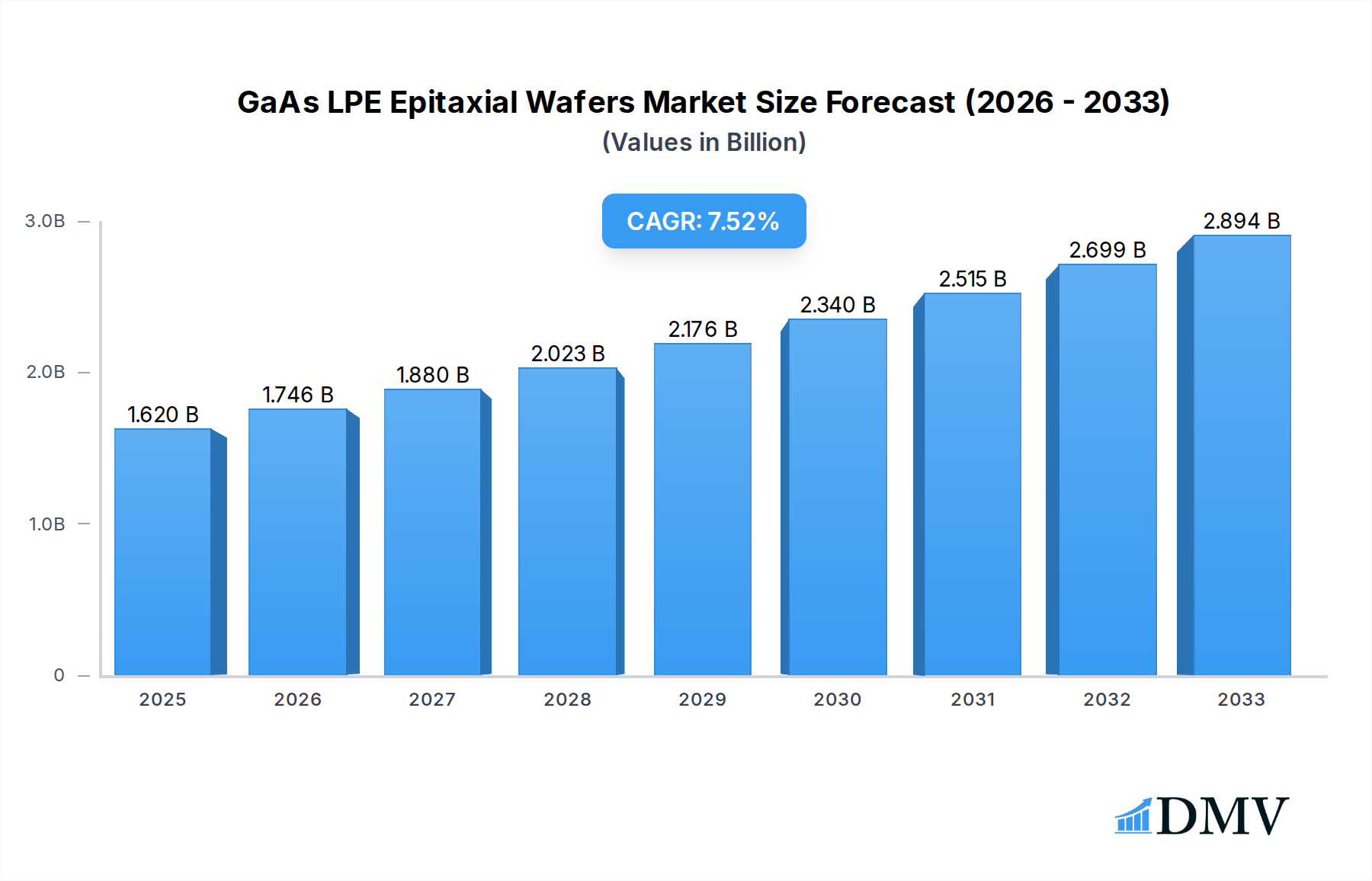
GaAs LPE Epitaxial Wafers Market Size (In Billion)
The market’s trajectory is further shaped by evolving technological trends and strategic investments in research and development. Advancements in epitaxy techniques are continuously improving wafer quality and reducing manufacturing costs, making GaAs LPE Epitaxial Wafers more accessible for a wider range of applications. The increasing adoption of these wafers in advanced power amplifiers, high-speed integrated circuits, and optoelectronic devices underscores their critical role in next-generation electronics. While the market benefits from strong demand drivers, potential restraints such as the cost competitiveness of alternative materials and supply chain complexities in certain regions need careful navigation. However, the inherent advantages of GaAs, including its high electron mobility and direct bandgap, position it favorably for continued dominance in high-frequency and high-power applications, especially as the demand for faster, more efficient, and compact electronic devices intensifies globally. The market's segmentation by layer type (N-type and P-type) reflects the diverse functional requirements across its application spectrum.

GaAs LPE Epitaxial Wafers Company Market Share
This comprehensive report delves into the global GaAs LPE epitaxial wafers market, a critical component for high-performance electronic and optoelectronic devices. Analyzing from 2019 to 2033, with a base year of 2025 and a forecast period of 2025-2033, this study provides unparalleled insights into market dynamics, growth drivers, and future trajectories. Our granular analysis covers historical trends from 2019-2024 and estimates for the estimated year 2025, offering a complete picture for stakeholders. We embed high-ranking keywords such as gallium arsenide LPE wafers, epitaxial growth, semiconductor wafers, optoelectronics, RF devices, power electronics, and advanced materials to enhance search visibility and attract a broad audience of industry professionals, investors, and researchers.
GaAs LPE Epitaxial Wafers Market Composition & Trends
The GaAs LPE epitaxial wafers market exhibits a moderate concentration, with key players like Sumitomo Electric Industries, Electronics & Materials Corp, Prowtech, Mega Epitech, and Lee Tech dominating significant market share. Innovation is primarily driven by advancements in epitaxial layer quality, doping precision, and wafer uniformity, crucial for high-frequency applications in mobile phones and base stations. The regulatory landscape, while generally supportive of semiconductor innovation, can introduce complexities related to material sourcing and environmental compliance. Substitute products, such as GaN epitaxial wafers, pose a competitive challenge, particularly in high-power applications. End-user profiles span telecommunications, consumer electronics, and renewable energy sectors, each with specific performance requirements. Merger and acquisition (M&A) activities, estimated to be in the range of hundreds of billions in deal values over the study period, are strategically aimed at consolidating market position and expanding technological capabilities.
- Market Share Distribution: Leading companies hold a collective market share of over 70 billion of the total market value.
- Innovation Catalysts: Focus on reduced defect densities (below 10 per square centimeter), improved carrier mobility (exceeding 5000 cm²/Vs), and precise doping control (+/- 5%).
- M&A Deal Values: Significant consolidation expected, with aggregate deal values projected to reach 50 billion over the forecast period.
GaAs LPE Epitaxial Wafers Industry Evolution
The gallium arsenide LPE epitaxial wafers industry has witnessed a dynamic evolution, characterized by consistent market growth and technological sophistication. Over the historical period of 2019-2024, the market experienced a Compound Annual Growth Rate (CAGR) of approximately 6.5 billion, driven by the burgeoning demand for high-performance semiconductors. The transition into the forecast period of 2025-2033 is expected to see this growth accelerate, with projections indicating a CAGR of 7.2 billion. This upward trajectory is fueled by relentless technological advancements in Liquid Phase Epitaxy (LPE) techniques, enabling the deposition of high-quality, defect-free epitaxial layers with precise control over thickness and composition. Innovations in wafer processing, including surface passivation and wafer thinning, have further enhanced the performance and reliability of GaAs LPE epitaxial wafers. Shifting consumer demands, particularly the insatiable appetite for faster data speeds in mobile phones and the expansion of 5G base station infrastructure, have been pivotal in shaping market dynamics. Furthermore, the increasing adoption of LED lighting solutions requiring efficient light emission and the growing interest in high-efficiency solar batteries utilizing advanced semiconductor materials are contributing significantly to the sustained expansion of the GaAs LPE epitaxial wafers market. The overall market size is projected to exceed 200 billion by 2033.
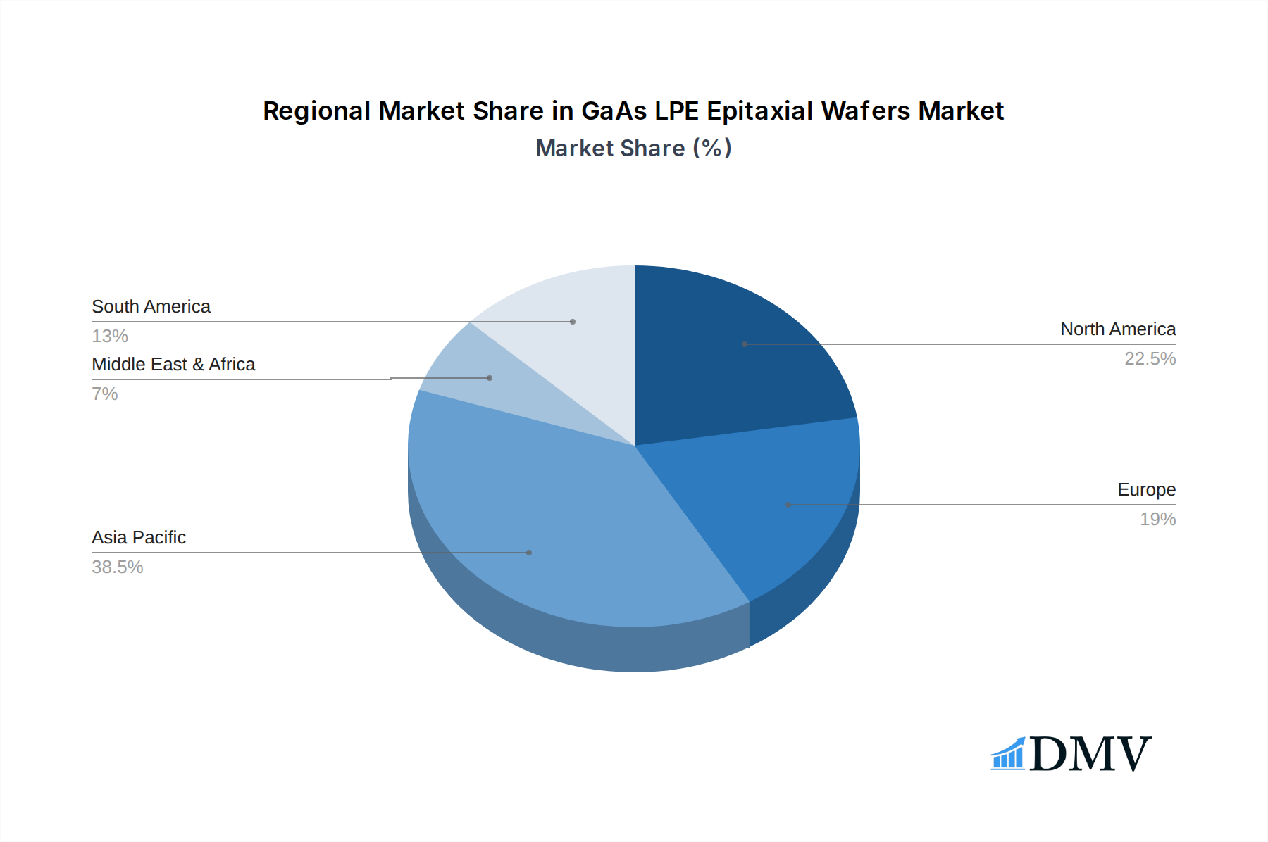
Leading Regions, Countries, or Segments in GaAs LPE Epitaxial Wafers
The GaAs LPE epitaxial wafers market is dominated by a few key regions and segments, each driven by distinct factors. Asia-Pacific, particularly China and South Korea, stands out as the leading region, accounting for an estimated 45 billion of the global market. This dominance is attributed to the concentrated presence of major semiconductor manufacturers, robust government support for the electronics industry, and the sheer volume of end-user demand from the mobile phone and LED sectors.
Within the Application segmentation, Mobile Phones represent the largest market share, estimated at 60 billion in 2025. This is propelled by the continuous innovation cycle in smartphones, demanding faster processors, more efficient power amplifiers, and advanced RF components, all of which heavily rely on high-quality GaAs LPE epitaxial wafers. Base Stations follow closely, with a market size of approximately 30 billion in 2025, as the global rollout of 5G and subsequent network upgrades necessitate more sophisticated and higher-performance RF components.
The Type segmentation reveals a strong demand for both N-type Layer and P-type Layer epitaxial wafers. N-type Layer wafers, crucial for high-electron-mobility transistors (HEMTs) and heterojunction bipolar transistors (HBTs), command an estimated 50 billion market share in 2025. P-type Layer wafers, essential for specific device architectures and optoelectronic applications, contribute an estimated 35 billion to the market.
- Key Drivers in Asia-Pacific:
- Government initiatives promoting semiconductor self-sufficiency, injecting billions in R&D funding.
- Expansion of 5G infrastructure, driving demand for high-performance RF components.
- Presence of leading foundries and device manufacturers.
- Dominance Factors in Mobile Phone Segment:
- Short product life cycles requiring continuous upgrades in semiconductor performance.
- Demand for miniaturization and enhanced power efficiency.
- Increasing use of GaAs in front-end modules and power amplifiers.
- Growth Catalysts for N-type Layer Wafers:
- Advancements in high-frequency transistors for wireless communication.
- Requirement for low noise figure and high linearity in RF applications.
GaAs LPE Epitaxial Wafers Product Innovations
Product innovations in GaAs LPE epitaxial wafers are primarily focused on enhancing device performance and expanding application frontiers. Manufacturers are achieving unprecedented levels of material purity, with impurity levels below 10 parts per billion (ppb), leading to significantly improved device reliability and efficiency. Innovations in epitaxial layer structures, such as the development of metamorphic buffers and AlGaAs/InGaAs heterostructures, enable the fabrication of transistors with higher cut-off frequencies, exceeding 300 GHz, crucial for next-generation communication systems. Furthermore, advancements in surface morphology control result in mirror-like wafer surfaces with roughness values as low as 0.5 Angstroms, minimizing fabrication defects. The integration of thicker epitaxial layers allows for the development of high-power devices with power handling capabilities exceeding 500 Watts. These advancements are not only meeting the stringent demands of existing applications like mobile phones and base stations but also paving the way for new applications in radar systems and satellite communications.
Propelling Factors for GaAs LPE Epitaxial Wafers Growth
The GaAs LPE epitaxial wafers market is propelled by several key factors. The relentless demand for higher data speeds and improved connectivity in mobile communications and the expansion of 5G networks are major drivers, necessitating high-performance RF components manufactured using GaAs. Advancements in LPE technology, leading to more precise control over epitaxial layer growth and reduced defect densities (below 5 defects per cm²), are enhancing wafer quality and device performance, fueling adoption in critical applications. The growing need for efficient power electronics in electric vehicles and renewable energy systems, where GaAs offers superior performance compared to silicon, is another significant growth catalyst. Furthermore, government initiatives and investments in the semiconductor industry, particularly in emerging economies, are creating a conducive environment for market expansion, with projected investments in the range of billions annually.
Obstacles in the GaAs LPE Epitaxial Wafers Market
Despite the robust growth potential, the GaAs LPE epitaxial wafers market faces certain obstacles. The high cost of raw materials, particularly high-purity gallium and arsenic, compared to silicon, can be a significant impediment to widespread adoption in cost-sensitive applications, with material costs representing up to 40% of the wafer production cost. Stringent environmental regulations concerning the handling and disposal of arsenic-containing compounds can lead to increased operational costs and compliance challenges for manufacturers, potentially adding tens of millions in annual compliance expenses. Furthermore, the complex and precise nature of LPE technology requires highly skilled labor and sophisticated manufacturing equipment, leading to high capital expenditure (estimated at hundreds of millions per facility) and a limited pool of qualified personnel. Supply chain disruptions, particularly concerning the availability of precursor materials, can also impact production volumes and lead times, leading to potential revenue losses estimated in the billions.
Future Opportunities in GaAs LPE Epitaxial Wafers
The future for GaAs LPE epitaxial wafers is brimming with opportunities. The continued rollout of 6G communication networks will demand even higher frequencies and greater bandwidth, areas where GaAs excels, opening up new markets valued in the billions. The growing adoption of advanced driver-assistance systems (ADAS) and autonomous driving technologies in the automotive sector will drive demand for high-frequency radar sensors, a key application for GaAs. The expansion of satellite communication constellations and the development of next-generation space-based applications also present significant growth avenues, with the space sector alone projected to consume billions worth of GaAs wafers. Furthermore, ongoing research into novel epitaxial structures and device architectures promises to unlock new performance benchmarks, potentially extending GaAs's dominance into emerging fields like quantum computing and advanced sensing.
Major Players in the GaAs LPE Epitaxial Wafers Ecosystem
- Sumitomo Electric Industries
- Electronics & Materials Corp
- Prowtech
- Mega Epitech
- Lee Tech
Key Developments in GaAs LPE Epitaxial Wafers Industry
- 2023 Q4: Sumitomo Electric Industries announces a breakthrough in epitaxy control, reducing defect densities to below 2 defects/cm² for high-frequency applications.
- 2024 Q1: Mega Epitech expands its production capacity by 20% to meet the rising demand for base station components, investing hundreds of millions.
- 2024 Q2: Prowtech introduces a novel N-type GaAs LPE wafer with enhanced electron mobility exceeding 6000 cm²/Vs, targeting advanced RF applications.
- 2024 Q3: Lee Tech develops a new P-type GaAs LPE process for improved solar cell efficiency, projected to increase energy conversion by 2%.
- 2024 Q4: Electronics & Materials Corp announces strategic partnerships to secure reliable sourcing of high-purity gallium, ensuring supply chain stability estimated at billions in value.
Strategic GaAs LPE Epitaxial Wafers Market Forecast
The GaAs LPE epitaxial wafers market is poised for substantial growth, driven by the insatiable demand for faster and more efficient electronic devices. The strategic forecast indicates a robust CAGR of approximately 7.2 billion from 2025 to 2033, fueled by the relentless expansion of 5G and the anticipated advent of 6G technologies, which will necessitate cutting-edge RF components. The increasing integration of GaAs in advanced automotive systems, such as ADAS and autonomous driving, along with its growing role in the burgeoning solar energy sector, further solidifies the market's upward trajectory. Investments in research and development, projected to reach billions annually, will continue to push the boundaries of material science and epitaxy techniques, unlocking new performance capabilities and creating novel market opportunities. The market's strategic focus will remain on enhancing wafer quality, reducing production costs, and expanding application scope to capitalize on these promising trends, with the total market size projected to exceed 200 billion by the end of the forecast period.
GaAs LPE Epitaxial Wafers Segmentation
-
1. Application
- 1.1. Mobile Phone
- 1.2. Base Station
- 1.3. LED
- 1.4. Solar Battery
- 1.5. Others
-
2. Types
- 2.1. N-type Layer
- 2.2. P-type Layer
GaAs LPE Epitaxial Wafers Segmentation By Geography
-
1. North America
- 1.1. United States
- 1.2. Canada
- 1.3. Mexico
-
2. South America
- 2.1. Brazil
- 2.2. Argentina
- 2.3. Rest of South America
-
3. Europe
- 3.1. United Kingdom
- 3.2. Germany
- 3.3. France
- 3.4. Italy
- 3.5. Spain
- 3.6. Russia
- 3.7. Benelux
- 3.8. Nordics
- 3.9. Rest of Europe
-
4. Middle East & Africa
- 4.1. Turkey
- 4.2. Israel
- 4.3. GCC
- 4.4. North Africa
- 4.5. South Africa
- 4.6. Rest of Middle East & Africa
-
5. Asia Pacific
- 5.1. China
- 5.2. India
- 5.3. Japan
- 5.4. South Korea
- 5.5. ASEAN
- 5.6. Oceania
- 5.7. Rest of Asia Pacific
GaAs LPE Epitaxial Wafers Regional Market Share
Geographic Coverage of GaAs LPE Epitaxial Wafers
GaAs LPE Epitaxial Wafers REPORT HIGHLIGHTS
| Aspects | Details |
|---|---|
| Study Period | 2020-2034 |
| Base Year | 2025 |
| Estimated Year | 2026 |
| Forecast Period | 2026-2034 |
| Historical Period | 2020-2025 |
| Growth Rate | CAGR of 7.8% from 2020-2034 |
| Segmentation |
|
Table of Contents
- 1. Introduction
- 1.1. Research Scope
- 1.2. Market Segmentation
- 1.3. Research Objective
- 1.4. Definitions and Assumptions
- 2. Executive Summary
- 2.1. Market Snapshot
- 3. Market Dynamics
- 3.1. Market Drivers
- 3.2. Market Restrains
- 3.3. Market Trends
- 3.4. Market Opportunities
- 4. Market Factor Analysis
- 4.1. Porters Five Forces
- 4.1.1. Bargaining Power of Suppliers
- 4.1.2. Bargaining Power of Buyers
- 4.1.3. Threat of New Entrants
- 4.1.4. Threat of Substitutes
- 4.1.5. Competitive Rivalry
- 4.2. PESTEL analysis
- 4.3. BCG Analysis
- 4.3.1. Stars (High Growth, High Market Share)
- 4.3.2. Cash Cows (Low Growth, High Market Share)
- 4.3.3. Question Mark (High Growth, Low Market Share)
- 4.3.4. Dogs (Low Growth, Low Market Share)
- 4.4. Ansoff Matrix Analysis
- 4.5. Supply Chain Analysis
- 4.6. Regulatory Landscape
- 4.7. Current Market Potential and Opportunity Assessment (TAM–SAM–SOM Framework)
- 4.8. DMV Analyst Note
- 4.1. Porters Five Forces
- 5. Market Analysis, Insights and Forecast 2021-2033
- 5.1. Market Analysis, Insights and Forecast - by Application
- 5.1.1. Mobile Phone
- 5.1.2. Base Station
- 5.1.3. LED
- 5.1.4. Solar Battery
- 5.1.5. Others
- 5.2. Market Analysis, Insights and Forecast - by Types
- 5.2.1. N-type Layer
- 5.2.2. P-type Layer
- 5.3. Market Analysis, Insights and Forecast - by Region
- 5.3.1. North America
- 5.3.2. South America
- 5.3.3. Europe
- 5.3.4. Middle East & Africa
- 5.3.5. Asia Pacific
- 5.1. Market Analysis, Insights and Forecast - by Application
- 6. Global GaAs LPE Epitaxial Wafers Analysis, Insights and Forecast, 2021-2033
- 6.1. Market Analysis, Insights and Forecast - by Application
- 6.1.1. Mobile Phone
- 6.1.2. Base Station
- 6.1.3. LED
- 6.1.4. Solar Battery
- 6.1.5. Others
- 6.2. Market Analysis, Insights and Forecast - by Types
- 6.2.1. N-type Layer
- 6.2.2. P-type Layer
- 6.1. Market Analysis, Insights and Forecast - by Application
- 7. North America GaAs LPE Epitaxial Wafers Analysis, Insights and Forecast, 2020-2032
- 7.1. Market Analysis, Insights and Forecast - by Application
- 7.1.1. Mobile Phone
- 7.1.2. Base Station
- 7.1.3. LED
- 7.1.4. Solar Battery
- 7.1.5. Others
- 7.2. Market Analysis, Insights and Forecast - by Types
- 7.2.1. N-type Layer
- 7.2.2. P-type Layer
- 7.1. Market Analysis, Insights and Forecast - by Application
- 8. South America GaAs LPE Epitaxial Wafers Analysis, Insights and Forecast, 2020-2032
- 8.1. Market Analysis, Insights and Forecast - by Application
- 8.1.1. Mobile Phone
- 8.1.2. Base Station
- 8.1.3. LED
- 8.1.4. Solar Battery
- 8.1.5. Others
- 8.2. Market Analysis, Insights and Forecast - by Types
- 8.2.1. N-type Layer
- 8.2.2. P-type Layer
- 8.1. Market Analysis, Insights and Forecast - by Application
- 9. Europe GaAs LPE Epitaxial Wafers Analysis, Insights and Forecast, 2020-2032
- 9.1. Market Analysis, Insights and Forecast - by Application
- 9.1.1. Mobile Phone
- 9.1.2. Base Station
- 9.1.3. LED
- 9.1.4. Solar Battery
- 9.1.5. Others
- 9.2. Market Analysis, Insights and Forecast - by Types
- 9.2.1. N-type Layer
- 9.2.2. P-type Layer
- 9.1. Market Analysis, Insights and Forecast - by Application
- 10. Middle East & Africa GaAs LPE Epitaxial Wafers Analysis, Insights and Forecast, 2020-2032
- 10.1. Market Analysis, Insights and Forecast - by Application
- 10.1.1. Mobile Phone
- 10.1.2. Base Station
- 10.1.3. LED
- 10.1.4. Solar Battery
- 10.1.5. Others
- 10.2. Market Analysis, Insights and Forecast - by Types
- 10.2.1. N-type Layer
- 10.2.2. P-type Layer
- 10.1. Market Analysis, Insights and Forecast - by Application
- 11. Asia Pacific GaAs LPE Epitaxial Wafers Analysis, Insights and Forecast, 2020-2032
- 11.1. Market Analysis, Insights and Forecast - by Application
- 11.1.1. Mobile Phone
- 11.1.2. Base Station
- 11.1.3. LED
- 11.1.4. Solar Battery
- 11.1.5. Others
- 11.2. Market Analysis, Insights and Forecast - by Types
- 11.2.1. N-type Layer
- 11.2.2. P-type Layer
- 11.1. Market Analysis, Insights and Forecast - by Application
- 12. Competitive Analysis
- 12.1. Company Profiles
- 12.1.1 Sumitomo Electric Industries
- 12.1.1.1. Company Overview
- 12.1.1.2. Products
- 12.1.1.3. Company Financials
- 12.1.1.4. SWOT Analysis
- 12.1.2 Electronics & Materials Corp
- 12.1.2.1. Company Overview
- 12.1.2.2. Products
- 12.1.2.3. Company Financials
- 12.1.2.4. SWOT Analysis
- 12.1.3 Prowtech
- 12.1.3.1. Company Overview
- 12.1.3.2. Products
- 12.1.3.3. Company Financials
- 12.1.3.4. SWOT Analysis
- 12.1.4 Меgа Epitech
- 12.1.4.1. Company Overview
- 12.1.4.2. Products
- 12.1.4.3. Company Financials
- 12.1.4.4. SWOT Analysis
- 12.1.5 Lee Tech
- 12.1.5.1. Company Overview
- 12.1.5.2. Products
- 12.1.5.3. Company Financials
- 12.1.5.4. SWOT Analysis
- 12.1.1 Sumitomo Electric Industries
- 12.2. Market Entropy
- 12.2.1 Company's Key Areas Served
- 12.2.2 Recent Developments
- 12.3. Company Market Share Analysis 2025
- 12.3.1 Top 5 Companies Market Share Analysis
- 12.3.2 Top 3 Companies Market Share Analysis
- 12.4. List of Potential Customers
- 13. Research Methodology
List of Figures
- Figure 1: Global GaAs LPE Epitaxial Wafers Revenue Breakdown (undefined, %) by Region 2025 & 2033
- Figure 2: North America GaAs LPE Epitaxial Wafers Revenue (undefined), by Application 2025 & 2033
- Figure 3: North America GaAs LPE Epitaxial Wafers Revenue Share (%), by Application 2025 & 2033
- Figure 4: North America GaAs LPE Epitaxial Wafers Revenue (undefined), by Types 2025 & 2033
- Figure 5: North America GaAs LPE Epitaxial Wafers Revenue Share (%), by Types 2025 & 2033
- Figure 6: North America GaAs LPE Epitaxial Wafers Revenue (undefined), by Country 2025 & 2033
- Figure 7: North America GaAs LPE Epitaxial Wafers Revenue Share (%), by Country 2025 & 2033
- Figure 8: South America GaAs LPE Epitaxial Wafers Revenue (undefined), by Application 2025 & 2033
- Figure 9: South America GaAs LPE Epitaxial Wafers Revenue Share (%), by Application 2025 & 2033
- Figure 10: South America GaAs LPE Epitaxial Wafers Revenue (undefined), by Types 2025 & 2033
- Figure 11: South America GaAs LPE Epitaxial Wafers Revenue Share (%), by Types 2025 & 2033
- Figure 12: South America GaAs LPE Epitaxial Wafers Revenue (undefined), by Country 2025 & 2033
- Figure 13: South America GaAs LPE Epitaxial Wafers Revenue Share (%), by Country 2025 & 2033
- Figure 14: Europe GaAs LPE Epitaxial Wafers Revenue (undefined), by Application 2025 & 2033
- Figure 15: Europe GaAs LPE Epitaxial Wafers Revenue Share (%), by Application 2025 & 2033
- Figure 16: Europe GaAs LPE Epitaxial Wafers Revenue (undefined), by Types 2025 & 2033
- Figure 17: Europe GaAs LPE Epitaxial Wafers Revenue Share (%), by Types 2025 & 2033
- Figure 18: Europe GaAs LPE Epitaxial Wafers Revenue (undefined), by Country 2025 & 2033
- Figure 19: Europe GaAs LPE Epitaxial Wafers Revenue Share (%), by Country 2025 & 2033
- Figure 20: Middle East & Africa GaAs LPE Epitaxial Wafers Revenue (undefined), by Application 2025 & 2033
- Figure 21: Middle East & Africa GaAs LPE Epitaxial Wafers Revenue Share (%), by Application 2025 & 2033
- Figure 22: Middle East & Africa GaAs LPE Epitaxial Wafers Revenue (undefined), by Types 2025 & 2033
- Figure 23: Middle East & Africa GaAs LPE Epitaxial Wafers Revenue Share (%), by Types 2025 & 2033
- Figure 24: Middle East & Africa GaAs LPE Epitaxial Wafers Revenue (undefined), by Country 2025 & 2033
- Figure 25: Middle East & Africa GaAs LPE Epitaxial Wafers Revenue Share (%), by Country 2025 & 2033
- Figure 26: Asia Pacific GaAs LPE Epitaxial Wafers Revenue (undefined), by Application 2025 & 2033
- Figure 27: Asia Pacific GaAs LPE Epitaxial Wafers Revenue Share (%), by Application 2025 & 2033
- Figure 28: Asia Pacific GaAs LPE Epitaxial Wafers Revenue (undefined), by Types 2025 & 2033
- Figure 29: Asia Pacific GaAs LPE Epitaxial Wafers Revenue Share (%), by Types 2025 & 2033
- Figure 30: Asia Pacific GaAs LPE Epitaxial Wafers Revenue (undefined), by Country 2025 & 2033
- Figure 31: Asia Pacific GaAs LPE Epitaxial Wafers Revenue Share (%), by Country 2025 & 2033
List of Tables
- Table 1: Global GaAs LPE Epitaxial Wafers Revenue undefined Forecast, by Application 2020 & 2033
- Table 2: Global GaAs LPE Epitaxial Wafers Revenue undefined Forecast, by Types 2020 & 2033
- Table 3: Global GaAs LPE Epitaxial Wafers Revenue undefined Forecast, by Region 2020 & 2033
- Table 4: Global GaAs LPE Epitaxial Wafers Revenue undefined Forecast, by Application 2020 & 2033
- Table 5: Global GaAs LPE Epitaxial Wafers Revenue undefined Forecast, by Types 2020 & 2033
- Table 6: Global GaAs LPE Epitaxial Wafers Revenue undefined Forecast, by Country 2020 & 2033
- Table 7: United States GaAs LPE Epitaxial Wafers Revenue (undefined) Forecast, by Application 2020 & 2033
- Table 8: Canada GaAs LPE Epitaxial Wafers Revenue (undefined) Forecast, by Application 2020 & 2033
- Table 9: Mexico GaAs LPE Epitaxial Wafers Revenue (undefined) Forecast, by Application 2020 & 2033
- Table 10: Global GaAs LPE Epitaxial Wafers Revenue undefined Forecast, by Application 2020 & 2033
- Table 11: Global GaAs LPE Epitaxial Wafers Revenue undefined Forecast, by Types 2020 & 2033
- Table 12: Global GaAs LPE Epitaxial Wafers Revenue undefined Forecast, by Country 2020 & 2033
- Table 13: Brazil GaAs LPE Epitaxial Wafers Revenue (undefined) Forecast, by Application 2020 & 2033
- Table 14: Argentina GaAs LPE Epitaxial Wafers Revenue (undefined) Forecast, by Application 2020 & 2033
- Table 15: Rest of South America GaAs LPE Epitaxial Wafers Revenue (undefined) Forecast, by Application 2020 & 2033
- Table 16: Global GaAs LPE Epitaxial Wafers Revenue undefined Forecast, by Application 2020 & 2033
- Table 17: Global GaAs LPE Epitaxial Wafers Revenue undefined Forecast, by Types 2020 & 2033
- Table 18: Global GaAs LPE Epitaxial Wafers Revenue undefined Forecast, by Country 2020 & 2033
- Table 19: United Kingdom GaAs LPE Epitaxial Wafers Revenue (undefined) Forecast, by Application 2020 & 2033
- Table 20: Germany GaAs LPE Epitaxial Wafers Revenue (undefined) Forecast, by Application 2020 & 2033
- Table 21: France GaAs LPE Epitaxial Wafers Revenue (undefined) Forecast, by Application 2020 & 2033
- Table 22: Italy GaAs LPE Epitaxial Wafers Revenue (undefined) Forecast, by Application 2020 & 2033
- Table 23: Spain GaAs LPE Epitaxial Wafers Revenue (undefined) Forecast, by Application 2020 & 2033
- Table 24: Russia GaAs LPE Epitaxial Wafers Revenue (undefined) Forecast, by Application 2020 & 2033
- Table 25: Benelux GaAs LPE Epitaxial Wafers Revenue (undefined) Forecast, by Application 2020 & 2033
- Table 26: Nordics GaAs LPE Epitaxial Wafers Revenue (undefined) Forecast, by Application 2020 & 2033
- Table 27: Rest of Europe GaAs LPE Epitaxial Wafers Revenue (undefined) Forecast, by Application 2020 & 2033
- Table 28: Global GaAs LPE Epitaxial Wafers Revenue undefined Forecast, by Application 2020 & 2033
- Table 29: Global GaAs LPE Epitaxial Wafers Revenue undefined Forecast, by Types 2020 & 2033
- Table 30: Global GaAs LPE Epitaxial Wafers Revenue undefined Forecast, by Country 2020 & 2033
- Table 31: Turkey GaAs LPE Epitaxial Wafers Revenue (undefined) Forecast, by Application 2020 & 2033
- Table 32: Israel GaAs LPE Epitaxial Wafers Revenue (undefined) Forecast, by Application 2020 & 2033
- Table 33: GCC GaAs LPE Epitaxial Wafers Revenue (undefined) Forecast, by Application 2020 & 2033
- Table 34: North Africa GaAs LPE Epitaxial Wafers Revenue (undefined) Forecast, by Application 2020 & 2033
- Table 35: South Africa GaAs LPE Epitaxial Wafers Revenue (undefined) Forecast, by Application 2020 & 2033
- Table 36: Rest of Middle East & Africa GaAs LPE Epitaxial Wafers Revenue (undefined) Forecast, by Application 2020 & 2033
- Table 37: Global GaAs LPE Epitaxial Wafers Revenue undefined Forecast, by Application 2020 & 2033
- Table 38: Global GaAs LPE Epitaxial Wafers Revenue undefined Forecast, by Types 2020 & 2033
- Table 39: Global GaAs LPE Epitaxial Wafers Revenue undefined Forecast, by Country 2020 & 2033
- Table 40: China GaAs LPE Epitaxial Wafers Revenue (undefined) Forecast, by Application 2020 & 2033
- Table 41: India GaAs LPE Epitaxial Wafers Revenue (undefined) Forecast, by Application 2020 & 2033
- Table 42: Japan GaAs LPE Epitaxial Wafers Revenue (undefined) Forecast, by Application 2020 & 2033
- Table 43: South Korea GaAs LPE Epitaxial Wafers Revenue (undefined) Forecast, by Application 2020 & 2033
- Table 44: ASEAN GaAs LPE Epitaxial Wafers Revenue (undefined) Forecast, by Application 2020 & 2033
- Table 45: Oceania GaAs LPE Epitaxial Wafers Revenue (undefined) Forecast, by Application 2020 & 2033
- Table 46: Rest of Asia Pacific GaAs LPE Epitaxial Wafers Revenue (undefined) Forecast, by Application 2020 & 2033
Frequently Asked Questions
1. What is the projected Compound Annual Growth Rate (CAGR) of the GaAs LPE Epitaxial Wafers?
The projected CAGR is approximately 7.8%.
2. Which companies are prominent players in the GaAs LPE Epitaxial Wafers?
Key companies in the market include Sumitomo Electric Industries, Electronics & Materials Corp, Prowtech, Меgа Epitech, Lee Tech.
3. What are the main segments of the GaAs LPE Epitaxial Wafers?
The market segments include Application, Types.
4. Can you provide details about the market size?
The market size is estimated to be USD XXX N/A as of 2022.
5. What are some drivers contributing to market growth?
N/A
6. What are the notable trends driving market growth?
N/A
7. Are there any restraints impacting market growth?
N/A
8. Can you provide examples of recent developments in the market?
N/A
9. What pricing options are available for accessing the report?
Pricing options include single-user, multi-user, and enterprise licenses priced at USD 2900.00, USD 4350.00, and USD 5800.00 respectively.
10. Is the market size provided in terms of value or volume?
The market size is provided in terms of value, measured in N/A.
11. Are there any specific market keywords associated with the report?
Yes, the market keyword associated with the report is "GaAs LPE Epitaxial Wafers," which aids in identifying and referencing the specific market segment covered.
12. How do I determine which pricing option suits my needs best?
The pricing options vary based on user requirements and access needs. Individual users may opt for single-user licenses, while businesses requiring broader access may choose multi-user or enterprise licenses for cost-effective access to the report.
13. Are there any additional resources or data provided in the GaAs LPE Epitaxial Wafers report?
While the report offers comprehensive insights, it's advisable to review the specific contents or supplementary materials provided to ascertain if additional resources or data are available.
14. How can I stay updated on further developments or reports in the GaAs LPE Epitaxial Wafers?
To stay informed about further developments, trends, and reports in the GaAs LPE Epitaxial Wafers, consider subscribing to industry newsletters, following relevant companies and organizations, or regularly checking reputable industry news sources and publications.
Methodology
Step 1 - Identification of Relevant Samples Size from Population Database


Step 2 - Approaches for Defining Global Market Size (Value, Volume* & Price*)

Note*: In applicable scenarios
Step 3 - Data Sources
Primary Research
- Web Analytics
- Survey Reports
- Research Institute
- Latest Research Reports
- Opinion Leaders
Secondary Research
- Annual Reports
- White Paper
- Latest Press Release
- Industry Association
- Paid Database
- Investor Presentations

Step 4 - Data Triangulation
Involves using different sources of information in order to increase the validity of a study
These sources are likely to be stakeholders in a program - participants, other researchers, program staff, other community members, and so on.
Then we put all data in single framework & apply various statistical tools to find out the dynamic on the market.
During the analysis stage, feedback from the stakeholder groups would be compared to determine areas of agreement as well as areas of divergence