

Key Insights
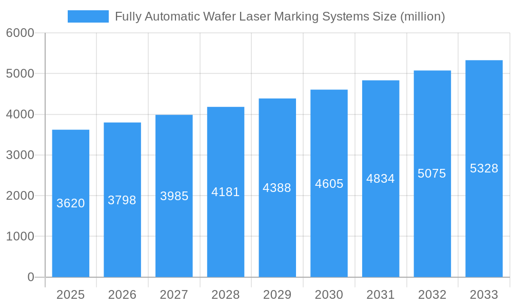
The Fully Automatic Wafer Laser Marking Systems market is poised for robust growth, projected to reach USD 3.62 billion in 2025, driven by an impressive CAGR of 4.82%. This expansion is primarily fueled by the increasing demand for sophisticated wafer identification and traceability solutions within the semiconductor industry. The miniaturization of electronic components and the growing complexity of semiconductor manufacturing processes necessitate highly precise and automated marking systems to ensure product integrity and efficient supply chain management. Key applications such as 300 mm and 200 mm wafer marking are expected to witness significant adoption, supported by advancements in laser technology that offer higher speed, improved accuracy, and enhanced flexibility for diverse marking requirements, including wafer back side and top side identification.
Fully Automatic Wafer Laser Marking Systems Market Size (In Billion)
The market's trajectory is further bolstered by emerging trends like the integration of artificial intelligence and machine learning into laser marking systems for enhanced quality control and predictive maintenance. Furthermore, the escalating need for counterfeit prevention and adherence to stringent industry regulations globally are significant growth catalysts. While the market benefits from strong demand, potential restraints such as the high initial investment cost of advanced systems and the availability of skilled labor for operation and maintenance might pose challenges. However, continuous innovation in laser sources and marking technologies, coupled with the expanding global semiconductor manufacturing footprint, particularly in Asia Pacific, is expected to outweigh these restraints, ensuring sustained market expansion throughout the forecast period.
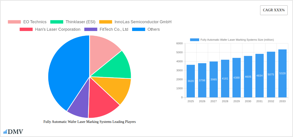
Fully Automatic Wafer Laser Marking Systems Company Market Share
Fully Automatic Wafer Laser Marking Systems Market Composition & Trends
The fully automatic wafer laser marking systems market is characterized by a moderate to high degree of concentration, with key players like EO Technics, Thinklaser (ESI), InnoLas Semiconductor GmbH, Han's Laser Corporation, and FitTech Co., Ltd. commanding significant market share. Innovation catalysts are predominantly driven by advancements in laser technology, enabling higher precision, faster marking speeds, and compatibility with an increasing range of wafer materials and sizes, including the rapidly growing 300 mm wafer segment. The regulatory landscape, particularly concerning semiconductor manufacturing standards and traceability requirements, plays a crucial role in shaping market demand. Substitute products, such as older etching or printing technologies, are progressively being phased out due to their lower efficiency and inability to meet stringent industry demands. End-user profiles primarily consist of semiconductor foundries, wafer fabrication plants, and integrated device manufacturers (IDMs) focused on enhancing production efficiency and product traceability. Mergers and acquisitions (M&A) activities, while not consistently at multi-billion dollar valuations for individual deals, are strategic in nature, aimed at consolidating market presence, expanding technological portfolios, and accessing new geographical markets. M&A deal values, where publicly disclosed, typically range from tens of millions to hundreds of millions of dollars, reflecting the specialized nature of this high-value industry segment. The market share distribution for key companies often fluctuates based on technological leadership and contract wins.
- Market Concentration: Moderate to High, driven by specialized technology and capital investment.
- Innovation Catalysts: Advanced laser sources (UV, picosecond, femtosecond), AI-driven process optimization, and integrated vision systems.
- Regulatory Landscapes: Semiconductor traceability mandates (e.g., SEMI standards), data integrity requirements.
- Substitute Products: Traditional etching, inkjet printing (limited applicability for high-precision wafer ID).
- End-User Profiles: Semiconductor fabrication plants, foundries, OSATs (Outsourced Semiconductor Assembly and Test).
- M&A Activities: Strategic acquisitions for technology enhancement and market reach.
Fully Automatic Wafer Laser Marking Systems Industry Evolution
The fully automatic wafer laser marking systems industry has undergone a transformative evolution, mirroring the rapid advancements and escalating demands within the global semiconductor sector. From its nascent stages of simpler, less integrated systems, the industry has matured into a sophisticated ecosystem driven by the need for ultra-precise, non-contact identification and tracking of semiconductor wafers throughout their complex manufacturing lifecycle. This evolution is intrinsically linked to the historical periods of intense research and development in laser technology, particularly the transition from traditional CO2 and YAG lasers to more advanced UV, picosecond, and femtosecond lasers, which offer superior resolution and minimal thermal impact on delicate wafer surfaces. The study period from 2019 to 2033 encapsulates a significant growth trajectory, marked by a compound annual growth rate (CAGR) that has consistently seen double-digit expansion, especially from 2019 to 2024, reflecting the burgeoning demand for semiconductors across diverse applications.
The base year of 2025 serves as a critical benchmark for understanding the current market state, with estimated figures for this year projected to show substantial growth from historical data. The forecast period from 2025 to 2033 is anticipated to witness sustained, robust growth, driven by several interconnected factors. The increasing complexity of semiconductor devices, the miniaturization of components, and the stringent requirements for traceability and quality control in advanced manufacturing processes necessitate highly accurate and reliable marking solutions. The 300 mm wafer segment, in particular, has been a primary driver of this growth, as larger wafer diameters offer greater cost efficiencies in production but also present unique challenges in terms of marking uniformity and defect avoidance.
Technological advancements have been at the forefront of this industry's evolution. Developments in laser beam steering, real-time in-situ process monitoring, and AI-powered defect detection have dramatically improved marking accuracy, speed, and the ability to mark on challenging surfaces, including wafer backside marking and intricate wafer ID marking. Consumer demand, in the broader sense of end-product sophistication and reliability, directly translates into the need for impeccable wafer-level identification and tracking. The increasing prevalence of IoT devices, AI-powered applications, and advanced automotive electronics has amplified the demand for high-performance semiconductors, thereby boosting the market for the sophisticated equipment required to produce them. Adoption metrics, such as the percentage of wafer lots processed by automated laser marking systems, have shown a significant upward trend, indicating a clear shift away from manual or less sophisticated methods. This sustained adoption, coupled with ongoing technological innovation and the increasing complexity of semiconductor manufacturing, paints a picture of an industry poised for continued expansion and refinement throughout the forecast period.
Leading Regions, Countries, or Segments in Fully Automatic Wafer Laser Marking Systems
The fully automatic wafer laser marking systems market is currently dominated by the 300 mm wafer segment, reflecting the industry's transition towards larger wafer diameters for enhanced manufacturing efficiency and cost-effectiveness. This dominance is underpinned by significant investment trends and robust technological adoption within regions leading semiconductor manufacturing.
- Application: 300 mm Wafer Dominance: The sheer volume of production for advanced semiconductor chips necessitates the use of 300 mm wafers. This segment benefits from economies of scale and is the primary focus for leading chip manufacturers and foundries. Consequently, the demand for highly precise and efficient laser marking systems capable of handling these larger wafers is exceptionally high. This includes both wafer back side marking for defect inspection and traceability, and wafer top side marker applications for intricate identification.
- Key Drivers for 300 mm Wafer Dominance:
- Investment Trends: Substantial capital expenditure by leading semiconductor companies on advanced fabrication facilities specifically equipped for 300 mm wafer processing. This includes billions of dollars invested annually in new fabs and upgrades to existing ones.
- Technological Advancement: The development of advanced laser marking technologies specifically tailored to the challenges of 300 mm wafers, such as uniform beam delivery across a larger surface area and minimal thermal stress.
- Regulatory Support: Industry standards, like those promulgated by SEMI, increasingly mandate precise and indelible marking for traceability and quality control, which are critical for high-volume 300 mm wafer production.
- Cost Efficiency: The inherent cost advantage of producing more chips per wafer drives the adoption of 300 mm technology, thereby fueling the demand for corresponding marking systems.
While the 300 mm wafer segment holds the current leadership, the Wafer ID Marker type is also a critical segment that complements the application dominance. The ability to embed unique, serialized identifiers on each wafer is paramount for supply chain management, counterfeit prevention, and detailed process tracking. This is especially true for high-value semiconductor components used in advanced electronics and critical infrastructure. The growth in IoT devices and the increasing complexity of integrated circuits have further amplified the need for robust wafer identification. Leading companies like EO Technics, Thinklaser (ESI), and InnoLas Semiconductor GmbH are at the forefront of developing sophisticated wafer ID marker systems.
Geographically, East Asia, particularly South Korea, Taiwan, and China, are major hubs for 300 mm wafer fabrication and consequently represent the largest markets for these laser marking systems. The United States and Europe also contribute significantly, driven by advanced R&D and specialized manufacturing capabilities. The continued expansion of the semiconductor industry, coupled with ongoing technological innovation in laser marking, ensures the sustained growth and dominance of the 300 mm wafer segment and the critical Wafer ID Marker type within the global market. The estimated market size for these systems is in the hundreds of billions, with the 300 mm wafer segment capturing a significant majority.
Fully Automatic Wafer Laser Marking Systems Product Innovations
Product innovations in fully automatic wafer laser marking systems are primarily focused on enhancing precision, speed, and versatility. Advanced laser sources, such as picosecond and femtosecond lasers, are enabling non-destructive marking with exceptionally high resolution, crucial for delicate wafer surfaces. Integration of AI and machine learning algorithms is improving defect detection and optimizing marking parameters in real-time, leading to higher yields. Innovations also include enhanced automation for robotic wafer handling, sophisticated vision systems for accurate positioning and verification, and modular system designs allowing for customization and future upgrades. These advancements ensure compatibility with a broader range of materials and wafer sizes, including 300 mm wafer applications, and support both wafer back side marker and wafer top side marker functionalities, along with highly secure wafer ID marker solutions.
Propelling Factors for Fully Automatic Wafer Laser Marking Systems Growth
The growth of the fully automatic wafer laser marking systems market is propelled by several key factors. Foremost is the escalating demand for semiconductors across diverse industries like automotive, consumer electronics, and AI, driving increased wafer production and thus the need for efficient marking. Technological advancements in laser technology, enabling higher precision and faster processing speeds, are critical. The increasing stringency of traceability requirements by regulatory bodies and the industry itself to ensure quality control and prevent counterfeiting is a significant driver. Furthermore, the shift towards larger wafer sizes, particularly 300 mm wafers, necessitates advanced marking solutions. Economic factors, including substantial investments by semiconductor manufacturers in upgrading their fabrication facilities, further contribute to market expansion. The estimated annual market growth is projected to be in the double digits, potentially exceeding fifteen percent.
Obstacles in the Fully Automatic Wafer Laser Marking Systems Market
Despite robust growth, the fully automatic wafer laser marking systems market faces several obstacles. The high initial capital investment required for these sophisticated systems can be a barrier for smaller manufacturers, with individual systems costing hundreds of thousands to millions of dollars. The supply chain for specialized laser components and high-purity materials can be subject to disruptions, impacting production timelines and costs. Rapid technological obsolescence necessitates continuous R&D investment, adding to operational expenses. Furthermore, the highly specialized nature of the workforce required to operate and maintain these advanced systems can pose recruitment and training challenges. Intense competition among established players and emerging entrants also creates pricing pressures.
Future Opportunities in Fully Automatic Wafer Laser Marking Systems
Future opportunities in the fully automatic wafer laser marking systems market are abundant, driven by emerging trends and technological frontiers. The growing demand for advanced packaging technologies, such as chiplets and 3D integration, will require novel marking solutions for intricate wafer structures. The expansion of semiconductor manufacturing into new geographical regions presents untapped market potential. Advancements in direct wafer writing technologies, beyond mere identification, for functional marking are also a promising area. The increasing adoption of AI for predictive maintenance and process optimization in laser marking systems will unlock further efficiencies. Emerging applications in specialized semiconductor sectors, like quantum computing and advanced sensor technology, will also create niche markets.
Major Players in the Fully Automatic Wafer Laser Marking Systems Ecosystem
- EO Technics
- Thinklaser (ESI)
- InnoLas Semiconductor GmbH
- Han's Laser Corporation
- FitTech Co., Ltd
- E&R Engineering Corp
- HANMI Semiconductor
- Towa Laserfront Corporation
- Genesem
- Hylax Technology
- Beijing KHL Technical Equipment
- Shenzhen D-WIN Technology
- Gem Laser Limited
- New Power Team Technology
- Nanjing Dinai Laser Technology
- Tianhong Laser
Key Developments in Fully Automatic Wafer Laser Marking Systems Industry
- 2023/2024: Increased adoption of picosecond and femtosecond laser technology for ultra-fine marking on advanced semiconductor wafers.
- 2022: Significant advancements in AI-driven defect detection and process optimization for wafer laser marking systems.
- 2021: Growing demand for integrated vision systems to enhance marking accuracy and verification for 300 mm wafer applications.
- 2020: Enhanced focus on robust wafer ID marker solutions to combat semiconductor counterfeit and improve supply chain traceability.
- 2019: Introduction of more modular and scalable laser marking system designs to cater to evolving manufacturing needs.
Strategic Fully Automatic Wafer Laser Marking Systems Market Forecast
The strategic forecast for the fully automatic wafer laser marking systems market is exceptionally positive, projected to experience robust growth in the billions over the forecast period. This expansion will be fueled by the continuous demand for semiconductors in advanced technologies, the ongoing transition to 300 mm wafer processing, and the imperative for enhanced traceability and quality control. Product innovations, particularly in laser technology and automation, will continue to be key growth catalysts. Emerging opportunities in new market segments and geographical regions, coupled with strategic alliances and potential M&A activities among key players, will further solidify market growth. The market's ability to adapt to evolving semiconductor manufacturing processes and stringent industry standards will be crucial for sustained success, with an estimated market value in the hundreds of billions by the end of the forecast period.
Fully Automatic Wafer Laser Marking Systems Segmentation
-
1. Application
- 1.1. 300 mm Wafer
- 1.2. 200 mm Wafer
- 1.3. Others
-
2. Type
- 2.1. Wafer Back Side Marker
- 2.2. Wafer Top Side Marker
- 2.3. Wafer ID Marker
Fully Automatic Wafer Laser Marking Systems Segmentation By Geography
-
1. North America
- 1.1. United States
- 1.2. Canada
- 1.3. Mexico
-
2. South America
- 2.1. Brazil
- 2.2. Argentina
- 2.3. Rest of South America
-
3. Europe
- 3.1. United Kingdom
- 3.2. Germany
- 3.3. France
- 3.4. Italy
- 3.5. Spain
- 3.6. Russia
- 3.7. Benelux
- 3.8. Nordics
- 3.9. Rest of Europe
-
4. Middle East & Africa
- 4.1. Turkey
- 4.2. Israel
- 4.3. GCC
- 4.4. North Africa
- 4.5. South Africa
- 4.6. Rest of Middle East & Africa
-
5. Asia Pacific
- 5.1. China
- 5.2. India
- 5.3. Japan
- 5.4. South Korea
- 5.5. ASEAN
- 5.6. Oceania
- 5.7. Rest of Asia Pacific
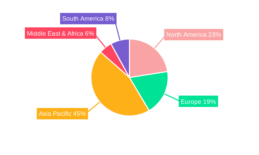
Fully Automatic Wafer Laser Marking Systems Regional Market Share
Geographic Coverage of Fully Automatic Wafer Laser Marking Systems
Fully Automatic Wafer Laser Marking Systems REPORT HIGHLIGHTS
| Aspects | Details |
|---|---|
| Study Period | 2020-2034 |
| Base Year | 2025 |
| Estimated Year | 2026 |
| Forecast Period | 2026-2034 |
| Historical Period | 2020-2025 |
| Growth Rate | CAGR of 9.4% from 2020-2034 |
| Segmentation |
|
Table of Contents
- 1. Introduction
- 1.1. Research Scope
- 1.2. Market Segmentation
- 1.3. Research Objective
- 1.4. Definitions and Assumptions
- 2. Executive Summary
- 2.1. Market Snapshot
- 3. Market Dynamics
- 3.1. Market Drivers
- 3.2. Market Restrains
- 3.3. Market Trends
- 3.4. Market Opportunities
- 4. Market Factor Analysis
- 4.1. Porters Five Forces
- 4.1.1. Bargaining Power of Suppliers
- 4.1.2. Bargaining Power of Buyers
- 4.1.3. Threat of New Entrants
- 4.1.4. Threat of Substitutes
- 4.1.5. Competitive Rivalry
- 4.2. PESTEL analysis
- 4.3. BCG Analysis
- 4.3.1. Stars (High Growth, High Market Share)
- 4.3.2. Cash Cows (Low Growth, High Market Share)
- 4.3.3. Question Mark (High Growth, Low Market Share)
- 4.3.4. Dogs (Low Growth, Low Market Share)
- 4.4. Ansoff Matrix Analysis
- 4.5. Supply Chain Analysis
- 4.6. Regulatory Landscape
- 4.7. Current Market Potential and Opportunity Assessment (TAM–SAM–SOM Framework)
- 4.8. DMV Analyst Note
- 4.1. Porters Five Forces
- 5. Market Analysis, Insights and Forecast 2021-2033
- 5.1. Market Analysis, Insights and Forecast - by Application
- 5.1.1. 300 mm Wafer
- 5.1.2. 200 mm Wafer
- 5.1.3. Others
- 5.2. Market Analysis, Insights and Forecast - by Type
- 5.2.1. Wafer Back Side Marker
- 5.2.2. Wafer Top Side Marker
- 5.2.3. Wafer ID Marker
- 5.3. Market Analysis, Insights and Forecast - by Region
- 5.3.1. North America
- 5.3.2. South America
- 5.3.3. Europe
- 5.3.4. Middle East & Africa
- 5.3.5. Asia Pacific
- 5.1. Market Analysis, Insights and Forecast - by Application
- 6. Global Fully Automatic Wafer Laser Marking Systems Analysis, Insights and Forecast, 2021-2033
- 6.1. Market Analysis, Insights and Forecast - by Application
- 6.1.1. 300 mm Wafer
- 6.1.2. 200 mm Wafer
- 6.1.3. Others
- 6.2. Market Analysis, Insights and Forecast - by Type
- 6.2.1. Wafer Back Side Marker
- 6.2.2. Wafer Top Side Marker
- 6.2.3. Wafer ID Marker
- 6.1. Market Analysis, Insights and Forecast - by Application
- 7. North America Fully Automatic Wafer Laser Marking Systems Analysis, Insights and Forecast, 2020-2032
- 7.1. Market Analysis, Insights and Forecast - by Application
- 7.1.1. 300 mm Wafer
- 7.1.2. 200 mm Wafer
- 7.1.3. Others
- 7.2. Market Analysis, Insights and Forecast - by Type
- 7.2.1. Wafer Back Side Marker
- 7.2.2. Wafer Top Side Marker
- 7.2.3. Wafer ID Marker
- 7.1. Market Analysis, Insights and Forecast - by Application
- 8. South America Fully Automatic Wafer Laser Marking Systems Analysis, Insights and Forecast, 2020-2032
- 8.1. Market Analysis, Insights and Forecast - by Application
- 8.1.1. 300 mm Wafer
- 8.1.2. 200 mm Wafer
- 8.1.3. Others
- 8.2. Market Analysis, Insights and Forecast - by Type
- 8.2.1. Wafer Back Side Marker
- 8.2.2. Wafer Top Side Marker
- 8.2.3. Wafer ID Marker
- 8.1. Market Analysis, Insights and Forecast - by Application
- 9. Europe Fully Automatic Wafer Laser Marking Systems Analysis, Insights and Forecast, 2020-2032
- 9.1. Market Analysis, Insights and Forecast - by Application
- 9.1.1. 300 mm Wafer
- 9.1.2. 200 mm Wafer
- 9.1.3. Others
- 9.2. Market Analysis, Insights and Forecast - by Type
- 9.2.1. Wafer Back Side Marker
- 9.2.2. Wafer Top Side Marker
- 9.2.3. Wafer ID Marker
- 9.1. Market Analysis, Insights and Forecast - by Application
- 10. Middle East & Africa Fully Automatic Wafer Laser Marking Systems Analysis, Insights and Forecast, 2020-2032
- 10.1. Market Analysis, Insights and Forecast - by Application
- 10.1.1. 300 mm Wafer
- 10.1.2. 200 mm Wafer
- 10.1.3. Others
- 10.2. Market Analysis, Insights and Forecast - by Type
- 10.2.1. Wafer Back Side Marker
- 10.2.2. Wafer Top Side Marker
- 10.2.3. Wafer ID Marker
- 10.1. Market Analysis, Insights and Forecast - by Application
- 11. Asia Pacific Fully Automatic Wafer Laser Marking Systems Analysis, Insights and Forecast, 2020-2032
- 11.1. Market Analysis, Insights and Forecast - by Application
- 11.1.1. 300 mm Wafer
- 11.1.2. 200 mm Wafer
- 11.1.3. Others
- 11.2. Market Analysis, Insights and Forecast - by Type
- 11.2.1. Wafer Back Side Marker
- 11.2.2. Wafer Top Side Marker
- 11.2.3. Wafer ID Marker
- 11.1. Market Analysis, Insights and Forecast - by Application
- 12. Competitive Analysis
- 12.1. Company Profiles
- 12.1.1 EO Technics
- 12.1.1.1. Company Overview
- 12.1.1.2. Products
- 12.1.1.3. Company Financials
- 12.1.1.4. SWOT Analysis
- 12.1.2 Thinklaser (ESI)
- 12.1.2.1. Company Overview
- 12.1.2.2. Products
- 12.1.2.3. Company Financials
- 12.1.2.4. SWOT Analysis
- 12.1.3 InnoLas Semiconductor GmbH
- 12.1.3.1. Company Overview
- 12.1.3.2. Products
- 12.1.3.3. Company Financials
- 12.1.3.4. SWOT Analysis
- 12.1.4 Han's Laser Corporation
- 12.1.4.1. Company Overview
- 12.1.4.2. Products
- 12.1.4.3. Company Financials
- 12.1.4.4. SWOT Analysis
- 12.1.5 FitTech Co. Ltd
- 12.1.5.1. Company Overview
- 12.1.5.2. Products
- 12.1.5.3. Company Financials
- 12.1.5.4. SWOT Analysis
- 12.1.6 E&R Engineering Corp
- 12.1.6.1. Company Overview
- 12.1.6.2. Products
- 12.1.6.3. Company Financials
- 12.1.6.4. SWOT Analysis
- 12.1.7 HANMI Semiconductor
- 12.1.7.1. Company Overview
- 12.1.7.2. Products
- 12.1.7.3. Company Financials
- 12.1.7.4. SWOT Analysis
- 12.1.8 Towa Laserfront Corporation
- 12.1.8.1. Company Overview
- 12.1.8.2. Products
- 12.1.8.3. Company Financials
- 12.1.8.4. SWOT Analysis
- 12.1.9 Genesem
- 12.1.9.1. Company Overview
- 12.1.9.2. Products
- 12.1.9.3. Company Financials
- 12.1.9.4. SWOT Analysis
- 12.1.10 Hylax Technology
- 12.1.10.1. Company Overview
- 12.1.10.2. Products
- 12.1.10.3. Company Financials
- 12.1.10.4. SWOT Analysis
- 12.1.11 Beijing KHL Technical Equipment
- 12.1.11.1. Company Overview
- 12.1.11.2. Products
- 12.1.11.3. Company Financials
- 12.1.11.4. SWOT Analysis
- 12.1.12 Shenzhen D-WIN Technology
- 12.1.12.1. Company Overview
- 12.1.12.2. Products
- 12.1.12.3. Company Financials
- 12.1.12.4. SWOT Analysis
- 12.1.13 Gem Laser Limited
- 12.1.13.1. Company Overview
- 12.1.13.2. Products
- 12.1.13.3. Company Financials
- 12.1.13.4. SWOT Analysis
- 12.1.14 New Power Team Technology
- 12.1.14.1. Company Overview
- 12.1.14.2. Products
- 12.1.14.3. Company Financials
- 12.1.14.4. SWOT Analysis
- 12.1.15 Nanjing Dinai Laser Technology
- 12.1.15.1. Company Overview
- 12.1.15.2. Products
- 12.1.15.3. Company Financials
- 12.1.15.4. SWOT Analysis
- 12.1.16 Tianhong Laser
- 12.1.16.1. Company Overview
- 12.1.16.2. Products
- 12.1.16.3. Company Financials
- 12.1.16.4. SWOT Analysis
- 12.1.1 EO Technics
- 12.2. Market Entropy
- 12.2.1 Company's Key Areas Served
- 12.2.2 Recent Developments
- 12.3. Company Market Share Analysis 2025
- 12.3.1 Top 5 Companies Market Share Analysis
- 12.3.2 Top 3 Companies Market Share Analysis
- 12.4. List of Potential Customers
- 13. Research Methodology
List of Figures
- Figure 1: Global Fully Automatic Wafer Laser Marking Systems Revenue Breakdown (undefined, %) by Region 2025 & 2033
- Figure 2: Global Fully Automatic Wafer Laser Marking Systems Volume Breakdown (K, %) by Region 2025 & 2033
- Figure 3: North America Fully Automatic Wafer Laser Marking Systems Revenue (undefined), by Application 2025 & 2033
- Figure 4: North America Fully Automatic Wafer Laser Marking Systems Volume (K), by Application 2025 & 2033
- Figure 5: North America Fully Automatic Wafer Laser Marking Systems Revenue Share (%), by Application 2025 & 2033
- Figure 6: North America Fully Automatic Wafer Laser Marking Systems Volume Share (%), by Application 2025 & 2033
- Figure 7: North America Fully Automatic Wafer Laser Marking Systems Revenue (undefined), by Type 2025 & 2033
- Figure 8: North America Fully Automatic Wafer Laser Marking Systems Volume (K), by Type 2025 & 2033
- Figure 9: North America Fully Automatic Wafer Laser Marking Systems Revenue Share (%), by Type 2025 & 2033
- Figure 10: North America Fully Automatic Wafer Laser Marking Systems Volume Share (%), by Type 2025 & 2033
- Figure 11: North America Fully Automatic Wafer Laser Marking Systems Revenue (undefined), by Country 2025 & 2033
- Figure 12: North America Fully Automatic Wafer Laser Marking Systems Volume (K), by Country 2025 & 2033
- Figure 13: North America Fully Automatic Wafer Laser Marking Systems Revenue Share (%), by Country 2025 & 2033
- Figure 14: North America Fully Automatic Wafer Laser Marking Systems Volume Share (%), by Country 2025 & 2033
- Figure 15: South America Fully Automatic Wafer Laser Marking Systems Revenue (undefined), by Application 2025 & 2033
- Figure 16: South America Fully Automatic Wafer Laser Marking Systems Volume (K), by Application 2025 & 2033
- Figure 17: South America Fully Automatic Wafer Laser Marking Systems Revenue Share (%), by Application 2025 & 2033
- Figure 18: South America Fully Automatic Wafer Laser Marking Systems Volume Share (%), by Application 2025 & 2033
- Figure 19: South America Fully Automatic Wafer Laser Marking Systems Revenue (undefined), by Type 2025 & 2033
- Figure 20: South America Fully Automatic Wafer Laser Marking Systems Volume (K), by Type 2025 & 2033
- Figure 21: South America Fully Automatic Wafer Laser Marking Systems Revenue Share (%), by Type 2025 & 2033
- Figure 22: South America Fully Automatic Wafer Laser Marking Systems Volume Share (%), by Type 2025 & 2033
- Figure 23: South America Fully Automatic Wafer Laser Marking Systems Revenue (undefined), by Country 2025 & 2033
- Figure 24: South America Fully Automatic Wafer Laser Marking Systems Volume (K), by Country 2025 & 2033
- Figure 25: South America Fully Automatic Wafer Laser Marking Systems Revenue Share (%), by Country 2025 & 2033
- Figure 26: South America Fully Automatic Wafer Laser Marking Systems Volume Share (%), by Country 2025 & 2033
- Figure 27: Europe Fully Automatic Wafer Laser Marking Systems Revenue (undefined), by Application 2025 & 2033
- Figure 28: Europe Fully Automatic Wafer Laser Marking Systems Volume (K), by Application 2025 & 2033
- Figure 29: Europe Fully Automatic Wafer Laser Marking Systems Revenue Share (%), by Application 2025 & 2033
- Figure 30: Europe Fully Automatic Wafer Laser Marking Systems Volume Share (%), by Application 2025 & 2033
- Figure 31: Europe Fully Automatic Wafer Laser Marking Systems Revenue (undefined), by Type 2025 & 2033
- Figure 32: Europe Fully Automatic Wafer Laser Marking Systems Volume (K), by Type 2025 & 2033
- Figure 33: Europe Fully Automatic Wafer Laser Marking Systems Revenue Share (%), by Type 2025 & 2033
- Figure 34: Europe Fully Automatic Wafer Laser Marking Systems Volume Share (%), by Type 2025 & 2033
- Figure 35: Europe Fully Automatic Wafer Laser Marking Systems Revenue (undefined), by Country 2025 & 2033
- Figure 36: Europe Fully Automatic Wafer Laser Marking Systems Volume (K), by Country 2025 & 2033
- Figure 37: Europe Fully Automatic Wafer Laser Marking Systems Revenue Share (%), by Country 2025 & 2033
- Figure 38: Europe Fully Automatic Wafer Laser Marking Systems Volume Share (%), by Country 2025 & 2033
- Figure 39: Middle East & Africa Fully Automatic Wafer Laser Marking Systems Revenue (undefined), by Application 2025 & 2033
- Figure 40: Middle East & Africa Fully Automatic Wafer Laser Marking Systems Volume (K), by Application 2025 & 2033
- Figure 41: Middle East & Africa Fully Automatic Wafer Laser Marking Systems Revenue Share (%), by Application 2025 & 2033
- Figure 42: Middle East & Africa Fully Automatic Wafer Laser Marking Systems Volume Share (%), by Application 2025 & 2033
- Figure 43: Middle East & Africa Fully Automatic Wafer Laser Marking Systems Revenue (undefined), by Type 2025 & 2033
- Figure 44: Middle East & Africa Fully Automatic Wafer Laser Marking Systems Volume (K), by Type 2025 & 2033
- Figure 45: Middle East & Africa Fully Automatic Wafer Laser Marking Systems Revenue Share (%), by Type 2025 & 2033
- Figure 46: Middle East & Africa Fully Automatic Wafer Laser Marking Systems Volume Share (%), by Type 2025 & 2033
- Figure 47: Middle East & Africa Fully Automatic Wafer Laser Marking Systems Revenue (undefined), by Country 2025 & 2033
- Figure 48: Middle East & Africa Fully Automatic Wafer Laser Marking Systems Volume (K), by Country 2025 & 2033
- Figure 49: Middle East & Africa Fully Automatic Wafer Laser Marking Systems Revenue Share (%), by Country 2025 & 2033
- Figure 50: Middle East & Africa Fully Automatic Wafer Laser Marking Systems Volume Share (%), by Country 2025 & 2033
- Figure 51: Asia Pacific Fully Automatic Wafer Laser Marking Systems Revenue (undefined), by Application 2025 & 2033
- Figure 52: Asia Pacific Fully Automatic Wafer Laser Marking Systems Volume (K), by Application 2025 & 2033
- Figure 53: Asia Pacific Fully Automatic Wafer Laser Marking Systems Revenue Share (%), by Application 2025 & 2033
- Figure 54: Asia Pacific Fully Automatic Wafer Laser Marking Systems Volume Share (%), by Application 2025 & 2033
- Figure 55: Asia Pacific Fully Automatic Wafer Laser Marking Systems Revenue (undefined), by Type 2025 & 2033
- Figure 56: Asia Pacific Fully Automatic Wafer Laser Marking Systems Volume (K), by Type 2025 & 2033
- Figure 57: Asia Pacific Fully Automatic Wafer Laser Marking Systems Revenue Share (%), by Type 2025 & 2033
- Figure 58: Asia Pacific Fully Automatic Wafer Laser Marking Systems Volume Share (%), by Type 2025 & 2033
- Figure 59: Asia Pacific Fully Automatic Wafer Laser Marking Systems Revenue (undefined), by Country 2025 & 2033
- Figure 60: Asia Pacific Fully Automatic Wafer Laser Marking Systems Volume (K), by Country 2025 & 2033
- Figure 61: Asia Pacific Fully Automatic Wafer Laser Marking Systems Revenue Share (%), by Country 2025 & 2033
- Figure 62: Asia Pacific Fully Automatic Wafer Laser Marking Systems Volume Share (%), by Country 2025 & 2033
List of Tables
- Table 1: Global Fully Automatic Wafer Laser Marking Systems Revenue undefined Forecast, by Application 2020 & 2033
- Table 2: Global Fully Automatic Wafer Laser Marking Systems Volume K Forecast, by Application 2020 & 2033
- Table 3: Global Fully Automatic Wafer Laser Marking Systems Revenue undefined Forecast, by Type 2020 & 2033
- Table 4: Global Fully Automatic Wafer Laser Marking Systems Volume K Forecast, by Type 2020 & 2033
- Table 5: Global Fully Automatic Wafer Laser Marking Systems Revenue undefined Forecast, by Region 2020 & 2033
- Table 6: Global Fully Automatic Wafer Laser Marking Systems Volume K Forecast, by Region 2020 & 2033
- Table 7: Global Fully Automatic Wafer Laser Marking Systems Revenue undefined Forecast, by Application 2020 & 2033
- Table 8: Global Fully Automatic Wafer Laser Marking Systems Volume K Forecast, by Application 2020 & 2033
- Table 9: Global Fully Automatic Wafer Laser Marking Systems Revenue undefined Forecast, by Type 2020 & 2033
- Table 10: Global Fully Automatic Wafer Laser Marking Systems Volume K Forecast, by Type 2020 & 2033
- Table 11: Global Fully Automatic Wafer Laser Marking Systems Revenue undefined Forecast, by Country 2020 & 2033
- Table 12: Global Fully Automatic Wafer Laser Marking Systems Volume K Forecast, by Country 2020 & 2033
- Table 13: United States Fully Automatic Wafer Laser Marking Systems Revenue (undefined) Forecast, by Application 2020 & 2033
- Table 14: United States Fully Automatic Wafer Laser Marking Systems Volume (K) Forecast, by Application 2020 & 2033
- Table 15: Canada Fully Automatic Wafer Laser Marking Systems Revenue (undefined) Forecast, by Application 2020 & 2033
- Table 16: Canada Fully Automatic Wafer Laser Marking Systems Volume (K) Forecast, by Application 2020 & 2033
- Table 17: Mexico Fully Automatic Wafer Laser Marking Systems Revenue (undefined) Forecast, by Application 2020 & 2033
- Table 18: Mexico Fully Automatic Wafer Laser Marking Systems Volume (K) Forecast, by Application 2020 & 2033
- Table 19: Global Fully Automatic Wafer Laser Marking Systems Revenue undefined Forecast, by Application 2020 & 2033
- Table 20: Global Fully Automatic Wafer Laser Marking Systems Volume K Forecast, by Application 2020 & 2033
- Table 21: Global Fully Automatic Wafer Laser Marking Systems Revenue undefined Forecast, by Type 2020 & 2033
- Table 22: Global Fully Automatic Wafer Laser Marking Systems Volume K Forecast, by Type 2020 & 2033
- Table 23: Global Fully Automatic Wafer Laser Marking Systems Revenue undefined Forecast, by Country 2020 & 2033
- Table 24: Global Fully Automatic Wafer Laser Marking Systems Volume K Forecast, by Country 2020 & 2033
- Table 25: Brazil Fully Automatic Wafer Laser Marking Systems Revenue (undefined) Forecast, by Application 2020 & 2033
- Table 26: Brazil Fully Automatic Wafer Laser Marking Systems Volume (K) Forecast, by Application 2020 & 2033
- Table 27: Argentina Fully Automatic Wafer Laser Marking Systems Revenue (undefined) Forecast, by Application 2020 & 2033
- Table 28: Argentina Fully Automatic Wafer Laser Marking Systems Volume (K) Forecast, by Application 2020 & 2033
- Table 29: Rest of South America Fully Automatic Wafer Laser Marking Systems Revenue (undefined) Forecast, by Application 2020 & 2033
- Table 30: Rest of South America Fully Automatic Wafer Laser Marking Systems Volume (K) Forecast, by Application 2020 & 2033
- Table 31: Global Fully Automatic Wafer Laser Marking Systems Revenue undefined Forecast, by Application 2020 & 2033
- Table 32: Global Fully Automatic Wafer Laser Marking Systems Volume K Forecast, by Application 2020 & 2033
- Table 33: Global Fully Automatic Wafer Laser Marking Systems Revenue undefined Forecast, by Type 2020 & 2033
- Table 34: Global Fully Automatic Wafer Laser Marking Systems Volume K Forecast, by Type 2020 & 2033
- Table 35: Global Fully Automatic Wafer Laser Marking Systems Revenue undefined Forecast, by Country 2020 & 2033
- Table 36: Global Fully Automatic Wafer Laser Marking Systems Volume K Forecast, by Country 2020 & 2033
- Table 37: United Kingdom Fully Automatic Wafer Laser Marking Systems Revenue (undefined) Forecast, by Application 2020 & 2033
- Table 38: United Kingdom Fully Automatic Wafer Laser Marking Systems Volume (K) Forecast, by Application 2020 & 2033
- Table 39: Germany Fully Automatic Wafer Laser Marking Systems Revenue (undefined) Forecast, by Application 2020 & 2033
- Table 40: Germany Fully Automatic Wafer Laser Marking Systems Volume (K) Forecast, by Application 2020 & 2033
- Table 41: France Fully Automatic Wafer Laser Marking Systems Revenue (undefined) Forecast, by Application 2020 & 2033
- Table 42: France Fully Automatic Wafer Laser Marking Systems Volume (K) Forecast, by Application 2020 & 2033
- Table 43: Italy Fully Automatic Wafer Laser Marking Systems Revenue (undefined) Forecast, by Application 2020 & 2033
- Table 44: Italy Fully Automatic Wafer Laser Marking Systems Volume (K) Forecast, by Application 2020 & 2033
- Table 45: Spain Fully Automatic Wafer Laser Marking Systems Revenue (undefined) Forecast, by Application 2020 & 2033
- Table 46: Spain Fully Automatic Wafer Laser Marking Systems Volume (K) Forecast, by Application 2020 & 2033
- Table 47: Russia Fully Automatic Wafer Laser Marking Systems Revenue (undefined) Forecast, by Application 2020 & 2033
- Table 48: Russia Fully Automatic Wafer Laser Marking Systems Volume (K) Forecast, by Application 2020 & 2033
- Table 49: Benelux Fully Automatic Wafer Laser Marking Systems Revenue (undefined) Forecast, by Application 2020 & 2033
- Table 50: Benelux Fully Automatic Wafer Laser Marking Systems Volume (K) Forecast, by Application 2020 & 2033
- Table 51: Nordics Fully Automatic Wafer Laser Marking Systems Revenue (undefined) Forecast, by Application 2020 & 2033
- Table 52: Nordics Fully Automatic Wafer Laser Marking Systems Volume (K) Forecast, by Application 2020 & 2033
- Table 53: Rest of Europe Fully Automatic Wafer Laser Marking Systems Revenue (undefined) Forecast, by Application 2020 & 2033
- Table 54: Rest of Europe Fully Automatic Wafer Laser Marking Systems Volume (K) Forecast, by Application 2020 & 2033
- Table 55: Global Fully Automatic Wafer Laser Marking Systems Revenue undefined Forecast, by Application 2020 & 2033
- Table 56: Global Fully Automatic Wafer Laser Marking Systems Volume K Forecast, by Application 2020 & 2033
- Table 57: Global Fully Automatic Wafer Laser Marking Systems Revenue undefined Forecast, by Type 2020 & 2033
- Table 58: Global Fully Automatic Wafer Laser Marking Systems Volume K Forecast, by Type 2020 & 2033
- Table 59: Global Fully Automatic Wafer Laser Marking Systems Revenue undefined Forecast, by Country 2020 & 2033
- Table 60: Global Fully Automatic Wafer Laser Marking Systems Volume K Forecast, by Country 2020 & 2033
- Table 61: Turkey Fully Automatic Wafer Laser Marking Systems Revenue (undefined) Forecast, by Application 2020 & 2033
- Table 62: Turkey Fully Automatic Wafer Laser Marking Systems Volume (K) Forecast, by Application 2020 & 2033
- Table 63: Israel Fully Automatic Wafer Laser Marking Systems Revenue (undefined) Forecast, by Application 2020 & 2033
- Table 64: Israel Fully Automatic Wafer Laser Marking Systems Volume (K) Forecast, by Application 2020 & 2033
- Table 65: GCC Fully Automatic Wafer Laser Marking Systems Revenue (undefined) Forecast, by Application 2020 & 2033
- Table 66: GCC Fully Automatic Wafer Laser Marking Systems Volume (K) Forecast, by Application 2020 & 2033
- Table 67: North Africa Fully Automatic Wafer Laser Marking Systems Revenue (undefined) Forecast, by Application 2020 & 2033
- Table 68: North Africa Fully Automatic Wafer Laser Marking Systems Volume (K) Forecast, by Application 2020 & 2033
- Table 69: South Africa Fully Automatic Wafer Laser Marking Systems Revenue (undefined) Forecast, by Application 2020 & 2033
- Table 70: South Africa Fully Automatic Wafer Laser Marking Systems Volume (K) Forecast, by Application 2020 & 2033
- Table 71: Rest of Middle East & Africa Fully Automatic Wafer Laser Marking Systems Revenue (undefined) Forecast, by Application 2020 & 2033
- Table 72: Rest of Middle East & Africa Fully Automatic Wafer Laser Marking Systems Volume (K) Forecast, by Application 2020 & 2033
- Table 73: Global Fully Automatic Wafer Laser Marking Systems Revenue undefined Forecast, by Application 2020 & 2033
- Table 74: Global Fully Automatic Wafer Laser Marking Systems Volume K Forecast, by Application 2020 & 2033
- Table 75: Global Fully Automatic Wafer Laser Marking Systems Revenue undefined Forecast, by Type 2020 & 2033
- Table 76: Global Fully Automatic Wafer Laser Marking Systems Volume K Forecast, by Type 2020 & 2033
- Table 77: Global Fully Automatic Wafer Laser Marking Systems Revenue undefined Forecast, by Country 2020 & 2033
- Table 78: Global Fully Automatic Wafer Laser Marking Systems Volume K Forecast, by Country 2020 & 2033
- Table 79: China Fully Automatic Wafer Laser Marking Systems Revenue (undefined) Forecast, by Application 2020 & 2033
- Table 80: China Fully Automatic Wafer Laser Marking Systems Volume (K) Forecast, by Application 2020 & 2033
- Table 81: India Fully Automatic Wafer Laser Marking Systems Revenue (undefined) Forecast, by Application 2020 & 2033
- Table 82: India Fully Automatic Wafer Laser Marking Systems Volume (K) Forecast, by Application 2020 & 2033
- Table 83: Japan Fully Automatic Wafer Laser Marking Systems Revenue (undefined) Forecast, by Application 2020 & 2033
- Table 84: Japan Fully Automatic Wafer Laser Marking Systems Volume (K) Forecast, by Application 2020 & 2033
- Table 85: South Korea Fully Automatic Wafer Laser Marking Systems Revenue (undefined) Forecast, by Application 2020 & 2033
- Table 86: South Korea Fully Automatic Wafer Laser Marking Systems Volume (K) Forecast, by Application 2020 & 2033
- Table 87: ASEAN Fully Automatic Wafer Laser Marking Systems Revenue (undefined) Forecast, by Application 2020 & 2033
- Table 88: ASEAN Fully Automatic Wafer Laser Marking Systems Volume (K) Forecast, by Application 2020 & 2033
- Table 89: Oceania Fully Automatic Wafer Laser Marking Systems Revenue (undefined) Forecast, by Application 2020 & 2033
- Table 90: Oceania Fully Automatic Wafer Laser Marking Systems Volume (K) Forecast, by Application 2020 & 2033
- Table 91: Rest of Asia Pacific Fully Automatic Wafer Laser Marking Systems Revenue (undefined) Forecast, by Application 2020 & 2033
- Table 92: Rest of Asia Pacific Fully Automatic Wafer Laser Marking Systems Volume (K) Forecast, by Application 2020 & 2033
Frequently Asked Questions
1. What is the projected Compound Annual Growth Rate (CAGR) of the Fully Automatic Wafer Laser Marking Systems?
The projected CAGR is approximately 9.4%.
2. Which companies are prominent players in the Fully Automatic Wafer Laser Marking Systems?
Key companies in the market include EO Technics, Thinklaser (ESI), InnoLas Semiconductor GmbH, Han's Laser Corporation, FitTech Co., Ltd, E&R Engineering Corp, HANMI Semiconductor, Towa Laserfront Corporation, Genesem, Hylax Technology, Beijing KHL Technical Equipment, Shenzhen D-WIN Technology, Gem Laser Limited, New Power Team Technology, Nanjing Dinai Laser Technology, Tianhong Laser.
3. What are the main segments of the Fully Automatic Wafer Laser Marking Systems?
The market segments include Application, Type.
4. Can you provide details about the market size?
The market size is estimated to be USD XXX N/A as of 2022.
5. What are some drivers contributing to market growth?
N/A
6. What are the notable trends driving market growth?
N/A
7. Are there any restraints impacting market growth?
N/A
8. Can you provide examples of recent developments in the market?
N/A
9. What pricing options are available for accessing the report?
Pricing options include single-user, multi-user, and enterprise licenses priced at USD 3950.00, USD 5925.00, and USD 7900.00 respectively.
10. Is the market size provided in terms of value or volume?
The market size is provided in terms of value, measured in N/A and volume, measured in K.
11. Are there any specific market keywords associated with the report?
Yes, the market keyword associated with the report is "Fully Automatic Wafer Laser Marking Systems," which aids in identifying and referencing the specific market segment covered.
12. How do I determine which pricing option suits my needs best?
The pricing options vary based on user requirements and access needs. Individual users may opt for single-user licenses, while businesses requiring broader access may choose multi-user or enterprise licenses for cost-effective access to the report.
13. Are there any additional resources or data provided in the Fully Automatic Wafer Laser Marking Systems report?
While the report offers comprehensive insights, it's advisable to review the specific contents or supplementary materials provided to ascertain if additional resources or data are available.
14. How can I stay updated on further developments or reports in the Fully Automatic Wafer Laser Marking Systems?
To stay informed about further developments, trends, and reports in the Fully Automatic Wafer Laser Marking Systems, consider subscribing to industry newsletters, following relevant companies and organizations, or regularly checking reputable industry news sources and publications.
Methodology
Step 1 - Identification of Relevant Samples Size from Population Database


Step 2 - Approaches for Defining Global Market Size (Value, Volume* & Price*)

Note*: In applicable scenarios
Step 3 - Data Sources
Primary Research
- Web Analytics
- Survey Reports
- Research Institute
- Latest Research Reports
- Opinion Leaders
Secondary Research
- Annual Reports
- White Paper
- Latest Press Release
- Industry Association
- Paid Database
- Investor Presentations

Step 4 - Data Triangulation
Involves using different sources of information in order to increase the validity of a study
These sources are likely to be stakeholders in a program - participants, other researchers, program staff, other community members, and so on.
Then we put all data in single framework & apply various statistical tools to find out the dynamic on the market.
During the analysis stage, feedback from the stakeholder groups would be compared to determine areas of agreement as well as areas of divergence