

Key Insights
The Bright Field Wafer Defect Inspection System market is poised for significant expansion, projected to reach $4.9 billion in 2025. This growth is driven by an impressive CAGR of 10.6% throughout the forecast period. The increasing demand for advanced semiconductor devices across a multitude of industries, including communication, consumer electronics, and automotive, is a primary catalyst. As miniaturization and complexity in chip manufacturing continue to escalate, the need for highly accurate and efficient defect detection systems becomes paramount to ensure product yield and reliability. Innovations in optical inspection technologies, coupled with advancements in artificial intelligence and machine learning for automated defect classification, are further bolstering market growth. These technological integrations enable faster, more precise identification of minute defects that were previously undetectable, thereby enhancing the overall quality control process in semiconductor fabrication.
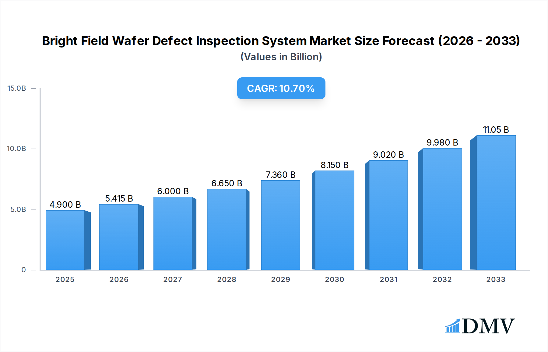
Bright Field Wafer Defect Inspection System Market Size (In Billion)
Key restraining factors for the market include the high initial investment required for sophisticated bright field inspection systems and the ongoing need for skilled personnel to operate and maintain them. The intricate nature of semiconductor manufacturing processes also presents challenges, demanding highly specialized inspection solutions that can adapt to evolving production techniques and materials. However, the pervasive trend towards smaller, more powerful electronic devices and the burgeoning adoption of IoT, 5G technology, and autonomous vehicles are creating an insatiable appetite for semiconductors. This surge in demand is compelling manufacturers to invest heavily in advanced inspection capabilities, overriding the aforementioned restraints. The market's segmentation by type reveals a strong focus on systems capable of detecting defects in the sub-10 nm range, reflecting the industry's push towards ever-smaller feature sizes in integrated circuits. Leading companies in this space are continuously innovating to meet these stringent requirements.

Bright Field Wafer Defect Inspection System Company Market Share
Bright Field Wafer Defect Inspection System Market Composition & Trends
The Bright Field Wafer Defect Inspection System market is characterized by a dynamic interplay of established giants and emerging innovators. Market concentration is moderately high, with key players like Onto Innovation Inc. and Nanotronics Imaging Inc. holding significant market shares. However, the proliferation of specialized solutions from companies such as TZTEK Technology Co., Ltd. and QES Mechatronic Sdn Bhd is fostering a competitive landscape. Innovation is primarily driven by the relentless demand for higher resolution inspection and automation in semiconductor manufacturing. Catalysts include the miniaturization of electronic components, the increasing complexity of wafer architectures, and the stringent quality control requirements across industries like Communication Device, Consumer Electronics, and Car Parts.
The regulatory landscape, while not overtly restrictive, emphasizes adherence to industry standards for semiconductor purity and defect detection. Substitute products, such as Dark Field inspection systems or Automated Optical Inspection (AOI) systems with different illumination techniques, exist but often cater to specific defect types or resolutions. End-user profiles are diverse, ranging from large-scale semiconductor foundries to specialized component manufacturers. Merger and acquisition (M&A) activities, though not at their peak, are strategic, aimed at consolidating technological capabilities or expanding market reach. For instance, potential M&A deal values in the semiconductor equipment sector have been in the range of several billion dollars in recent years.
- Market Share Distribution: Dominant players like Onto Innovation Inc. and Nanotronics Imaging Inc. command an estimated 60% of the market share in the historical period, with specialized players contributing the remaining 40%.
- M&A Deal Values: Recent strategic acquisitions in the broader semiconductor inspection market have seen valuations reaching upwards of 5 billion dollars, indicating investor confidence in the sector's growth.
- Innovation Catalysts: Miniaturization of transistors, 3D NAND and advanced packaging technologies, and AI-driven defect classification are key drivers of innovation.
- End-User Industries: Consumer Electronics (accounting for approximately 45% of demand), Communication Device (around 30%), and Car Parts (estimated 15%) are primary consumers.
Bright Field Wafer Defect Inspection System Industry Evolution
The Bright Field Wafer Defect Inspection System industry has undergone a significant evolutionary journey, driven by relentless technological advancements and the ever-increasing demands of the semiconductor ecosystem. The historical period from 2019 to 2024 witnessed a steady growth trajectory, propelled by the foundational need for precise defect identification on semiconductor wafers. During this phase, market growth rates averaged around 7% annually, a testament to the critical role these systems play in ensuring the quality and reliability of microelectronic components.
Technological advancements have been the cornerstone of this evolution. Early iterations of bright field inspection systems focused on macro-level defect detection. However, the market has progressively shifted towards ultra-high resolution capabilities, enabling the identification of sub-nanometer defects. This has been facilitated by innovations in optical microscopy, advanced sensor technologies, and sophisticated image processing algorithms. The adoption of machine learning and artificial intelligence (AI) for automated defect classification and root cause analysis has also been a transformative development, significantly enhancing inspection speed and accuracy. AI-driven anomaly detection has become a critical feature, allowing for the identification of previously unknown defect types.
Shifting consumer demands have further amplified this evolution. The proliferation of 5G technology, the explosive growth of the Internet of Things (IoT), and the increasing integration of advanced driver-assistance systems (ADAS) in vehicles have all necessitated higher performance and smaller form factors for electronic components. This translates directly into a greater need for defect-free wafers, pushing the boundaries of wafer inspection technology. The Consumer Electronics segment, particularly the demand for smartphones and advanced computing devices, has been a consistent driver, demanding wafers with defect densities below 10 parts per billion (ppb). Similarly, the Communication Device sector, driven by the rollout of 5G infrastructure and the increasing complexity of communication chips, requires defect-free wafers for optimal performance and signal integrity.
Furthermore, the evolution has also seen a greater emphasis on throughput and cost-effectiveness. Manufacturers are no longer satisfied with just accurate detection; they require systems that can inspect wafers at high speeds without compromising on precision, thereby reducing manufacturing costs and increasing overall yield. This has led to the development of parallel processing capabilities and optimized inspection routines. The integration of bright field inspection systems into fully automated production lines, minimizing human intervention and potential contamination, is another significant trend. The market for wafer defect inspection systems is projected to see sustained growth, with estimated CAGR of 8.5% between 2025 and 2033, reaching a market size exceeding 15 billion dollars by the end of the forecast period. The base year of 2025 is anticipated to see market revenues in the range of 9 billion dollars.
Leading Regions, Countries, or Segments in Bright Field Wafer Defect Inspection System
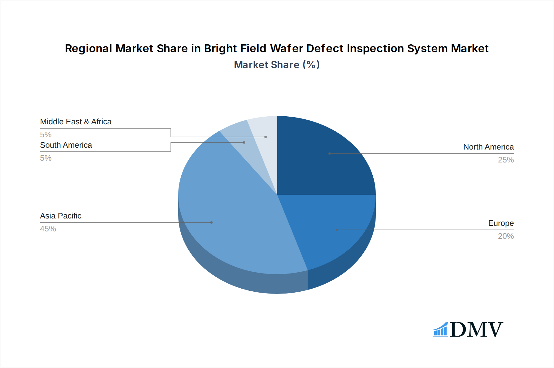
The global Bright Field Wafer Defect Inspection System market's dominance is intricately linked to the epicenters of semiconductor manufacturing and advanced electronics production. While numerous regions contribute to the demand, Asia Pacific consistently emerges as the leading region, driven by its substantial manufacturing base and increasing investments in cutting-edge semiconductor technologies. Within Asia Pacific, countries like South Korea, Taiwan, and China are at the forefront, housing major foundries and fabless semiconductor companies that are the primary consumers of these sophisticated inspection systems. The surge in demand from the Communication Device segment, particularly for 5G infrastructure and advanced mobile processors, has been a significant contributor to this regional dominance. This segment alone is estimated to account for 35% of the total market demand in the forecast period.
The Consumer Electronics segment, encompassing smartphones, tablets, and other smart devices, also plays a pivotal role in Asia Pacific's market leadership. The sheer volume of production for these devices necessitates high-throughput, accurate wafer defect inspection. This segment is projected to contribute approximately 40% to the overall market revenue during the study period. Investment trends in this region are particularly noteworthy. Governments in countries like China have been actively promoting domestic semiconductor manufacturing capabilities, leading to substantial investments in advanced equipment, including bright field wafer defect inspection systems. These government initiatives, often backed by billions in funding, create a fertile ground for market expansion.
When examining by Type, the segment of 1 nm to 10 nm defects is experiencing the most rapid growth and commands significant market attention. As device geometries continue to shrink, the ability to detect and characterize these minuscule defects becomes paramount. This specific type of inspection is crucial for advanced logic chips and memory devices, where even sub-nanometer imperfections can lead to device failure. The demand for inspection systems capable of resolving defects in the Less than 1 nm range is also on the rise, albeit from a smaller base, driven by the most advanced research and development in next-generation semiconductor technologies. The More than 10 nm segment, while still substantial, is witnessing slower growth as industry focus shifts towards ever-smaller defect detection.
Regulatory support in the form of incentives for semiconductor manufacturing and R&D also bolsters the market in these leading regions. Furthermore, the presence of key players like TZTEK Technology Co., Ltd. and QES Mechatronic Sdn Bhd, who are strategically positioned to serve the Asian market, further solidifies its leading status. The overall market size in Asia Pacific is projected to exceed 7 billion dollars by 2033.
- Dominant Region: Asia Pacific, driven by South Korea, Taiwan, and China.
- Key Applications: Communication Device (approx. 35% market share) and Consumer Electronics (approx. 40% market share).
- Leading Defect Type: 1 nm to 10 nm defects, crucial for advanced semiconductor nodes.
- Investment Trends: Significant government funding in semiconductor manufacturing infrastructure, exceeding 5 billion dollars annually in key Asian countries.
- Competitive Landscape: Strong presence of both global leaders and localized specialized providers.
Bright Field Wafer Defect Inspection System Product Innovations
Product innovations in bright field wafer defect inspection systems are continuously pushing the boundaries of resolution, speed, and intelligence. Recent advancements include the integration of ultra-high numerical aperture (NA) optics and advanced computational imaging techniques to achieve unprecedented defect detection sensitivity, capable of identifying defects smaller than 1 nm. These systems are now incorporating AI-powered algorithms for real-time anomaly detection and classification, reducing false positives and accelerating root cause analysis. Furthermore, enhanced throughput achieved through parallel inspection paths and optimized data processing allows for the inspection of billions of individual wafer sites within hours. These innovations are critical for the stringent quality demands of Communication Device and Consumer Electronics applications, ensuring reliable performance for billions of integrated circuits.
Propelling Factors for Bright Field Wafer Defect Inspection System Growth
The growth of the Bright Field Wafer Defect Inspection System market is propelled by several synergistic factors. The relentless drive towards miniaturization in semiconductor technology, exemplified by the progression to smaller nanometer nodes like 1 nm to 10 nm, necessitates more sensitive inspection capabilities. The booming demand for advanced electronic devices across Consumer Electronics, Communication Device, and Car Parts sectors fuels the need for higher wafer yields and defect-free components, driving investments in cutting-edge inspection equipment. Furthermore, government initiatives and substantial financial incentives, often in the billions of dollars, in key semiconductor manufacturing regions, particularly in Asia Pacific, are directly stimulating the adoption of these advanced systems. The increasing complexity of wafer designs and the adoption of novel materials also create new challenges that bright field inspection systems are uniquely positioned to address.
Obstacles in the Bright Field Wafer Defect Inspection System Market
Despite robust growth, the Bright Field Wafer Defect Inspection System market faces several obstacles. The extremely high cost of advanced inspection systems, often running into several million dollars per unit, can be a significant barrier for smaller manufacturers or those in developing regions. The rapid pace of technological evolution also presents a challenge, requiring continuous investment in upgrades and new equipment to remain competitive, potentially leading to rapid obsolescence. Supply chain disruptions, particularly for specialized components and raw materials, can impact manufacturing timelines and costs. Furthermore, the highly specialized nature of defect analysis and the shortage of skilled personnel capable of operating and maintaining these sophisticated systems pose ongoing challenges to widespread adoption and optimal utilization across the diverse segments.
Future Opportunities in Bright Field Wafer Defect Inspection System
The future of the Bright Field Wafer Defect Inspection System market is replete with opportunities, driven by emerging trends and technological frontiers. The increasing adoption of advanced packaging techniques and heterogeneous integration presents new inspection challenges and opportunities for bright field systems to identify defects in complex 3D structures. The expansion of the Car Parts segment, with its growing reliance on sophisticated semiconductors for autonomous driving and infotainment systems, offers a significant untapped market. Furthermore, the integration of advanced AI and machine learning models is expected to evolve from mere classification to predictive maintenance and proactive quality control, creating opportunities for smarter, more autonomous inspection solutions. The exploration of novel illumination and detection techniques, potentially enabling sub-angstrom defect detection, also represents a long-term opportunity for market leaders to redefine inspection standards, potentially supporting the development of devices with trillions of transistors.
Major Players in the Bright Field Wafer Defect Inspection System Ecosystem
- Nanotronics Imaging Inc.
- Onto Innovation Inc.
- C&D Semiconductor, Inc.
- TZTEK Technology Co., Ltd.
- NextIn Solutions
- InnoLas Semiconductor GmbH
- QES Mechatronic Sdn Bhd
- Mue Tec
- Acculex Solutions Pte. Ltd.
Key Developments in Bright Field Wafer Defect Inspection System Industry
- 2023/Q3: Nanotronics Imaging Inc. launched an AI-powered defect inspection platform, offering enhanced resolution and faster data analysis, impacting defect detection for Communication Device components.
- 2023/Q4: Onto Innovation Inc. announced significant advancements in their bright field inspection technology, focusing on sub-nanometer defect detection for next-generation memory chips, impacting the Consumer Electronics segment.
- 2024/Q1: TZTEK Technology Co., Ltd. introduced a new bright field inspection system with improved throughput, targeting the growing Car Parts semiconductor market.
- 2024/Q2: Mue Tec expanded its product portfolio with a solution optimized for inspecting wafers with complex 3D structures, addressing a key trend in advanced packaging.
- 2024/Q3: QES Mechatronic Sdn Bhd reported a substantial increase in adoption of their bright field inspection systems in Southeast Asian semiconductor manufacturing hubs, driven by demand from Consumer Electronics production.
Strategic Bright Field Wafer Defect Inspection System Market Forecast
The strategic forecast for the Bright Field Wafer Defect Inspection System market is exceptionally promising, projecting sustained growth driven by foundational industry needs and emerging technological paradigms. The continuous push for smaller geometries, particularly within the 1 nm to 10 nm defect detection range, will remain a primary growth catalyst. The burgeoning demand from the Communication Device, Consumer Electronics, and Car Parts sectors, all requiring increasingly sophisticated and defect-free semiconductors, will fuel significant market expansion. Strategic investments, government support in key manufacturing regions, and ongoing innovation in AI-driven inspection will further bolster market potential. The market is poised to see substantial growth, with an estimated compound annual growth rate of 8.5% from 2025 to 2033, reaching a valuation of over 15 billion dollars by the end of the forecast period.
Bright Field Wafer Defect Inspection System Segmentation
-
1. Application
- 1.1. Communication Device
- 1.2. Consumer Electronics
- 1.3. Car Parts
- 1.4. Others
-
2. Type
- 2.1. Less than 1 nm
- 2.2. 1 nm to 10 nm
- 2.3. More than 10 nm
- 2.4. Others
Bright Field Wafer Defect Inspection System Segmentation By Geography
-
1. North America
- 1.1. United States
- 1.2. Canada
- 1.3. Mexico
-
2. South America
- 2.1. Brazil
- 2.2. Argentina
- 2.3. Rest of South America
-
3. Europe
- 3.1. United Kingdom
- 3.2. Germany
- 3.3. France
- 3.4. Italy
- 3.5. Spain
- 3.6. Russia
- 3.7. Benelux
- 3.8. Nordics
- 3.9. Rest of Europe
-
4. Middle East & Africa
- 4.1. Turkey
- 4.2. Israel
- 4.3. GCC
- 4.4. North Africa
- 4.5. South Africa
- 4.6. Rest of Middle East & Africa
-
5. Asia Pacific
- 5.1. China
- 5.2. India
- 5.3. Japan
- 5.4. South Korea
- 5.5. ASEAN
- 5.6. Oceania
- 5.7. Rest of Asia Pacific
Bright Field Wafer Defect Inspection System Regional Market Share
Geographic Coverage of Bright Field Wafer Defect Inspection System
Bright Field Wafer Defect Inspection System REPORT HIGHLIGHTS
| Aspects | Details |
|---|---|
| Study Period | 2020-2034 |
| Base Year | 2025 |
| Estimated Year | 2026 |
| Forecast Period | 2026-2034 |
| Historical Period | 2020-2025 |
| Growth Rate | CAGR of 10.6% from 2020-2034 |
| Segmentation |
|
Table of Contents
- 1. Introduction
- 1.1. Research Scope
- 1.2. Market Segmentation
- 1.3. Research Objective
- 1.4. Definitions and Assumptions
- 2. Executive Summary
- 2.1. Market Snapshot
- 3. Market Dynamics
- 3.1. Market Drivers
- 3.2. Market Restrains
- 3.3. Market Trends
- 3.4. Market Opportunities
- 4. Market Factor Analysis
- 4.1. Porters Five Forces
- 4.1.1. Bargaining Power of Suppliers
- 4.1.2. Bargaining Power of Buyers
- 4.1.3. Threat of New Entrants
- 4.1.4. Threat of Substitutes
- 4.1.5. Competitive Rivalry
- 4.2. PESTEL analysis
- 4.3. BCG Analysis
- 4.3.1. Stars (High Growth, High Market Share)
- 4.3.2. Cash Cows (Low Growth, High Market Share)
- 4.3.3. Question Mark (High Growth, Low Market Share)
- 4.3.4. Dogs (Low Growth, Low Market Share)
- 4.4. Ansoff Matrix Analysis
- 4.5. Supply Chain Analysis
- 4.6. Regulatory Landscape
- 4.7. Current Market Potential and Opportunity Assessment (TAM–SAM–SOM Framework)
- 4.8. DMV Analyst Note
- 4.1. Porters Five Forces
- 5. Market Analysis, Insights and Forecast 2021-2033
- 5.1. Market Analysis, Insights and Forecast - by Application
- 5.1.1. Communication Device
- 5.1.2. Consumer Electronics
- 5.1.3. Car Parts
- 5.1.4. Others
- 5.2. Market Analysis, Insights and Forecast - by Type
- 5.2.1. Less than 1 nm
- 5.2.2. 1 nm to 10 nm
- 5.2.3. More than 10 nm
- 5.2.4. Others
- 5.3. Market Analysis, Insights and Forecast - by Region
- 5.3.1. North America
- 5.3.2. South America
- 5.3.3. Europe
- 5.3.4. Middle East & Africa
- 5.3.5. Asia Pacific
- 5.1. Market Analysis, Insights and Forecast - by Application
- 6. Global Bright Field Wafer Defect Inspection System Analysis, Insights and Forecast, 2021-2033
- 6.1. Market Analysis, Insights and Forecast - by Application
- 6.1.1. Communication Device
- 6.1.2. Consumer Electronics
- 6.1.3. Car Parts
- 6.1.4. Others
- 6.2. Market Analysis, Insights and Forecast - by Type
- 6.2.1. Less than 1 nm
- 6.2.2. 1 nm to 10 nm
- 6.2.3. More than 10 nm
- 6.2.4. Others
- 6.1. Market Analysis, Insights and Forecast - by Application
- 7. North America Bright Field Wafer Defect Inspection System Analysis, Insights and Forecast, 2020-2032
- 7.1. Market Analysis, Insights and Forecast - by Application
- 7.1.1. Communication Device
- 7.1.2. Consumer Electronics
- 7.1.3. Car Parts
- 7.1.4. Others
- 7.2. Market Analysis, Insights and Forecast - by Type
- 7.2.1. Less than 1 nm
- 7.2.2. 1 nm to 10 nm
- 7.2.3. More than 10 nm
- 7.2.4. Others
- 7.1. Market Analysis, Insights and Forecast - by Application
- 8. South America Bright Field Wafer Defect Inspection System Analysis, Insights and Forecast, 2020-2032
- 8.1. Market Analysis, Insights and Forecast - by Application
- 8.1.1. Communication Device
- 8.1.2. Consumer Electronics
- 8.1.3. Car Parts
- 8.1.4. Others
- 8.2. Market Analysis, Insights and Forecast - by Type
- 8.2.1. Less than 1 nm
- 8.2.2. 1 nm to 10 nm
- 8.2.3. More than 10 nm
- 8.2.4. Others
- 8.1. Market Analysis, Insights and Forecast - by Application
- 9. Europe Bright Field Wafer Defect Inspection System Analysis, Insights and Forecast, 2020-2032
- 9.1. Market Analysis, Insights and Forecast - by Application
- 9.1.1. Communication Device
- 9.1.2. Consumer Electronics
- 9.1.3. Car Parts
- 9.1.4. Others
- 9.2. Market Analysis, Insights and Forecast - by Type
- 9.2.1. Less than 1 nm
- 9.2.2. 1 nm to 10 nm
- 9.2.3. More than 10 nm
- 9.2.4. Others
- 9.1. Market Analysis, Insights and Forecast - by Application
- 10. Middle East & Africa Bright Field Wafer Defect Inspection System Analysis, Insights and Forecast, 2020-2032
- 10.1. Market Analysis, Insights and Forecast - by Application
- 10.1.1. Communication Device
- 10.1.2. Consumer Electronics
- 10.1.3. Car Parts
- 10.1.4. Others
- 10.2. Market Analysis, Insights and Forecast - by Type
- 10.2.1. Less than 1 nm
- 10.2.2. 1 nm to 10 nm
- 10.2.3. More than 10 nm
- 10.2.4. Others
- 10.1. Market Analysis, Insights and Forecast - by Application
- 11. Asia Pacific Bright Field Wafer Defect Inspection System Analysis, Insights and Forecast, 2020-2032
- 11.1. Market Analysis, Insights and Forecast - by Application
- 11.1.1. Communication Device
- 11.1.2. Consumer Electronics
- 11.1.3. Car Parts
- 11.1.4. Others
- 11.2. Market Analysis, Insights and Forecast - by Type
- 11.2.1. Less than 1 nm
- 11.2.2. 1 nm to 10 nm
- 11.2.3. More than 10 nm
- 11.2.4. Others
- 11.1. Market Analysis, Insights and Forecast - by Application
- 12. Competitive Analysis
- 12.1. Company Profiles
- 12.1.1 Nanotronics Imaging Inc.
- 12.1.1.1. Company Overview
- 12.1.1.2. Products
- 12.1.1.3. Company Financials
- 12.1.1.4. SWOT Analysis
- 12.1.2 Onto Innovation Inc.
- 12.1.2.1. Company Overview
- 12.1.2.2. Products
- 12.1.2.3. Company Financials
- 12.1.2.4. SWOT Analysis
- 12.1.3 C&D Semiconductor Inc.
- 12.1.3.1. Company Overview
- 12.1.3.2. Products
- 12.1.3.3. Company Financials
- 12.1.3.4. SWOT Analysis
- 12.1.4 TZTEK Technology Co. Ltd.
- 12.1.4.1. Company Overview
- 12.1.4.2. Products
- 12.1.4.3. Company Financials
- 12.1.4.4. SWOT Analysis
- 12.1.5 NextIn Solutions
- 12.1.5.1. Company Overview
- 12.1.5.2. Products
- 12.1.5.3. Company Financials
- 12.1.5.4. SWOT Analysis
- 12.1.6 InnoLas Semiconductor GmbH
- 12.1.6.1. Company Overview
- 12.1.6.2. Products
- 12.1.6.3. Company Financials
- 12.1.6.4. SWOT Analysis
- 12.1.7 QES Mechatronic Sdn Bhd
- 12.1.7.1. Company Overview
- 12.1.7.2. Products
- 12.1.7.3. Company Financials
- 12.1.7.4. SWOT Analysis
- 12.1.8 Mue Tec
- 12.1.8.1. Company Overview
- 12.1.8.2. Products
- 12.1.8.3. Company Financials
- 12.1.8.4. SWOT Analysis
- 12.1.9 Acculex Solutions Pte. Ltd.
- 12.1.9.1. Company Overview
- 12.1.9.2. Products
- 12.1.9.3. Company Financials
- 12.1.9.4. SWOT Analysis
- 12.1.1 Nanotronics Imaging Inc.
- 12.2. Market Entropy
- 12.2.1 Company's Key Areas Served
- 12.2.2 Recent Developments
- 12.3. Company Market Share Analysis 2025
- 12.3.1 Top 5 Companies Market Share Analysis
- 12.3.2 Top 3 Companies Market Share Analysis
- 12.4. List of Potential Customers
- 13. Research Methodology
List of Figures
- Figure 1: Global Bright Field Wafer Defect Inspection System Revenue Breakdown (undefined, %) by Region 2025 & 2033
- Figure 2: North America Bright Field Wafer Defect Inspection System Revenue (undefined), by Application 2025 & 2033
- Figure 3: North America Bright Field Wafer Defect Inspection System Revenue Share (%), by Application 2025 & 2033
- Figure 4: North America Bright Field Wafer Defect Inspection System Revenue (undefined), by Type 2025 & 2033
- Figure 5: North America Bright Field Wafer Defect Inspection System Revenue Share (%), by Type 2025 & 2033
- Figure 6: North America Bright Field Wafer Defect Inspection System Revenue (undefined), by Country 2025 & 2033
- Figure 7: North America Bright Field Wafer Defect Inspection System Revenue Share (%), by Country 2025 & 2033
- Figure 8: South America Bright Field Wafer Defect Inspection System Revenue (undefined), by Application 2025 & 2033
- Figure 9: South America Bright Field Wafer Defect Inspection System Revenue Share (%), by Application 2025 & 2033
- Figure 10: South America Bright Field Wafer Defect Inspection System Revenue (undefined), by Type 2025 & 2033
- Figure 11: South America Bright Field Wafer Defect Inspection System Revenue Share (%), by Type 2025 & 2033
- Figure 12: South America Bright Field Wafer Defect Inspection System Revenue (undefined), by Country 2025 & 2033
- Figure 13: South America Bright Field Wafer Defect Inspection System Revenue Share (%), by Country 2025 & 2033
- Figure 14: Europe Bright Field Wafer Defect Inspection System Revenue (undefined), by Application 2025 & 2033
- Figure 15: Europe Bright Field Wafer Defect Inspection System Revenue Share (%), by Application 2025 & 2033
- Figure 16: Europe Bright Field Wafer Defect Inspection System Revenue (undefined), by Type 2025 & 2033
- Figure 17: Europe Bright Field Wafer Defect Inspection System Revenue Share (%), by Type 2025 & 2033
- Figure 18: Europe Bright Field Wafer Defect Inspection System Revenue (undefined), by Country 2025 & 2033
- Figure 19: Europe Bright Field Wafer Defect Inspection System Revenue Share (%), by Country 2025 & 2033
- Figure 20: Middle East & Africa Bright Field Wafer Defect Inspection System Revenue (undefined), by Application 2025 & 2033
- Figure 21: Middle East & Africa Bright Field Wafer Defect Inspection System Revenue Share (%), by Application 2025 & 2033
- Figure 22: Middle East & Africa Bright Field Wafer Defect Inspection System Revenue (undefined), by Type 2025 & 2033
- Figure 23: Middle East & Africa Bright Field Wafer Defect Inspection System Revenue Share (%), by Type 2025 & 2033
- Figure 24: Middle East & Africa Bright Field Wafer Defect Inspection System Revenue (undefined), by Country 2025 & 2033
- Figure 25: Middle East & Africa Bright Field Wafer Defect Inspection System Revenue Share (%), by Country 2025 & 2033
- Figure 26: Asia Pacific Bright Field Wafer Defect Inspection System Revenue (undefined), by Application 2025 & 2033
- Figure 27: Asia Pacific Bright Field Wafer Defect Inspection System Revenue Share (%), by Application 2025 & 2033
- Figure 28: Asia Pacific Bright Field Wafer Defect Inspection System Revenue (undefined), by Type 2025 & 2033
- Figure 29: Asia Pacific Bright Field Wafer Defect Inspection System Revenue Share (%), by Type 2025 & 2033
- Figure 30: Asia Pacific Bright Field Wafer Defect Inspection System Revenue (undefined), by Country 2025 & 2033
- Figure 31: Asia Pacific Bright Field Wafer Defect Inspection System Revenue Share (%), by Country 2025 & 2033
List of Tables
- Table 1: Global Bright Field Wafer Defect Inspection System Revenue undefined Forecast, by Application 2020 & 2033
- Table 2: Global Bright Field Wafer Defect Inspection System Revenue undefined Forecast, by Type 2020 & 2033
- Table 3: Global Bright Field Wafer Defect Inspection System Revenue undefined Forecast, by Region 2020 & 2033
- Table 4: Global Bright Field Wafer Defect Inspection System Revenue undefined Forecast, by Application 2020 & 2033
- Table 5: Global Bright Field Wafer Defect Inspection System Revenue undefined Forecast, by Type 2020 & 2033
- Table 6: Global Bright Field Wafer Defect Inspection System Revenue undefined Forecast, by Country 2020 & 2033
- Table 7: United States Bright Field Wafer Defect Inspection System Revenue (undefined) Forecast, by Application 2020 & 2033
- Table 8: Canada Bright Field Wafer Defect Inspection System Revenue (undefined) Forecast, by Application 2020 & 2033
- Table 9: Mexico Bright Field Wafer Defect Inspection System Revenue (undefined) Forecast, by Application 2020 & 2033
- Table 10: Global Bright Field Wafer Defect Inspection System Revenue undefined Forecast, by Application 2020 & 2033
- Table 11: Global Bright Field Wafer Defect Inspection System Revenue undefined Forecast, by Type 2020 & 2033
- Table 12: Global Bright Field Wafer Defect Inspection System Revenue undefined Forecast, by Country 2020 & 2033
- Table 13: Brazil Bright Field Wafer Defect Inspection System Revenue (undefined) Forecast, by Application 2020 & 2033
- Table 14: Argentina Bright Field Wafer Defect Inspection System Revenue (undefined) Forecast, by Application 2020 & 2033
- Table 15: Rest of South America Bright Field Wafer Defect Inspection System Revenue (undefined) Forecast, by Application 2020 & 2033
- Table 16: Global Bright Field Wafer Defect Inspection System Revenue undefined Forecast, by Application 2020 & 2033
- Table 17: Global Bright Field Wafer Defect Inspection System Revenue undefined Forecast, by Type 2020 & 2033
- Table 18: Global Bright Field Wafer Defect Inspection System Revenue undefined Forecast, by Country 2020 & 2033
- Table 19: United Kingdom Bright Field Wafer Defect Inspection System Revenue (undefined) Forecast, by Application 2020 & 2033
- Table 20: Germany Bright Field Wafer Defect Inspection System Revenue (undefined) Forecast, by Application 2020 & 2033
- Table 21: France Bright Field Wafer Defect Inspection System Revenue (undefined) Forecast, by Application 2020 & 2033
- Table 22: Italy Bright Field Wafer Defect Inspection System Revenue (undefined) Forecast, by Application 2020 & 2033
- Table 23: Spain Bright Field Wafer Defect Inspection System Revenue (undefined) Forecast, by Application 2020 & 2033
- Table 24: Russia Bright Field Wafer Defect Inspection System Revenue (undefined) Forecast, by Application 2020 & 2033
- Table 25: Benelux Bright Field Wafer Defect Inspection System Revenue (undefined) Forecast, by Application 2020 & 2033
- Table 26: Nordics Bright Field Wafer Defect Inspection System Revenue (undefined) Forecast, by Application 2020 & 2033
- Table 27: Rest of Europe Bright Field Wafer Defect Inspection System Revenue (undefined) Forecast, by Application 2020 & 2033
- Table 28: Global Bright Field Wafer Defect Inspection System Revenue undefined Forecast, by Application 2020 & 2033
- Table 29: Global Bright Field Wafer Defect Inspection System Revenue undefined Forecast, by Type 2020 & 2033
- Table 30: Global Bright Field Wafer Defect Inspection System Revenue undefined Forecast, by Country 2020 & 2033
- Table 31: Turkey Bright Field Wafer Defect Inspection System Revenue (undefined) Forecast, by Application 2020 & 2033
- Table 32: Israel Bright Field Wafer Defect Inspection System Revenue (undefined) Forecast, by Application 2020 & 2033
- Table 33: GCC Bright Field Wafer Defect Inspection System Revenue (undefined) Forecast, by Application 2020 & 2033
- Table 34: North Africa Bright Field Wafer Defect Inspection System Revenue (undefined) Forecast, by Application 2020 & 2033
- Table 35: South Africa Bright Field Wafer Defect Inspection System Revenue (undefined) Forecast, by Application 2020 & 2033
- Table 36: Rest of Middle East & Africa Bright Field Wafer Defect Inspection System Revenue (undefined) Forecast, by Application 2020 & 2033
- Table 37: Global Bright Field Wafer Defect Inspection System Revenue undefined Forecast, by Application 2020 & 2033
- Table 38: Global Bright Field Wafer Defect Inspection System Revenue undefined Forecast, by Type 2020 & 2033
- Table 39: Global Bright Field Wafer Defect Inspection System Revenue undefined Forecast, by Country 2020 & 2033
- Table 40: China Bright Field Wafer Defect Inspection System Revenue (undefined) Forecast, by Application 2020 & 2033
- Table 41: India Bright Field Wafer Defect Inspection System Revenue (undefined) Forecast, by Application 2020 & 2033
- Table 42: Japan Bright Field Wafer Defect Inspection System Revenue (undefined) Forecast, by Application 2020 & 2033
- Table 43: South Korea Bright Field Wafer Defect Inspection System Revenue (undefined) Forecast, by Application 2020 & 2033
- Table 44: ASEAN Bright Field Wafer Defect Inspection System Revenue (undefined) Forecast, by Application 2020 & 2033
- Table 45: Oceania Bright Field Wafer Defect Inspection System Revenue (undefined) Forecast, by Application 2020 & 2033
- Table 46: Rest of Asia Pacific Bright Field Wafer Defect Inspection System Revenue (undefined) Forecast, by Application 2020 & 2033
Frequently Asked Questions
1. What is the projected Compound Annual Growth Rate (CAGR) of the Bright Field Wafer Defect Inspection System?
The projected CAGR is approximately 10.6%.
2. Which companies are prominent players in the Bright Field Wafer Defect Inspection System?
Key companies in the market include Nanotronics Imaging Inc., Onto Innovation Inc., C&D Semiconductor, Inc., TZTEK Technology Co., Ltd., NextIn Solutions, InnoLas Semiconductor GmbH, QES Mechatronic Sdn Bhd, Mue Tec, Acculex Solutions Pte. Ltd..
3. What are the main segments of the Bright Field Wafer Defect Inspection System?
The market segments include Application, Type.
4. Can you provide details about the market size?
The market size is estimated to be USD XXX N/A as of 2022.
5. What are some drivers contributing to market growth?
N/A
6. What are the notable trends driving market growth?
N/A
7. Are there any restraints impacting market growth?
N/A
8. Can you provide examples of recent developments in the market?
N/A
9. What pricing options are available for accessing the report?
Pricing options include single-user, multi-user, and enterprise licenses priced at USD 2900.00, USD 4350.00, and USD 5800.00 respectively.
10. Is the market size provided in terms of value or volume?
The market size is provided in terms of value, measured in N/A.
11. Are there any specific market keywords associated with the report?
Yes, the market keyword associated with the report is "Bright Field Wafer Defect Inspection System," which aids in identifying and referencing the specific market segment covered.
12. How do I determine which pricing option suits my needs best?
The pricing options vary based on user requirements and access needs. Individual users may opt for single-user licenses, while businesses requiring broader access may choose multi-user or enterprise licenses for cost-effective access to the report.
13. Are there any additional resources or data provided in the Bright Field Wafer Defect Inspection System report?
While the report offers comprehensive insights, it's advisable to review the specific contents or supplementary materials provided to ascertain if additional resources or data are available.
14. How can I stay updated on further developments or reports in the Bright Field Wafer Defect Inspection System?
To stay informed about further developments, trends, and reports in the Bright Field Wafer Defect Inspection System, consider subscribing to industry newsletters, following relevant companies and organizations, or regularly checking reputable industry news sources and publications.
Methodology
Step 1 - Identification of Relevant Samples Size from Population Database


Step 2 - Approaches for Defining Global Market Size (Value, Volume* & Price*)

Note*: In applicable scenarios
Step 3 - Data Sources
Primary Research
- Web Analytics
- Survey Reports
- Research Institute
- Latest Research Reports
- Opinion Leaders
Secondary Research
- Annual Reports
- White Paper
- Latest Press Release
- Industry Association
- Paid Database
- Investor Presentations

Step 4 - Data Triangulation
Involves using different sources of information in order to increase the validity of a study
These sources are likely to be stakeholders in a program - participants, other researchers, program staff, other community members, and so on.
Then we put all data in single framework & apply various statistical tools to find out the dynamic on the market.
During the analysis stage, feedback from the stakeholder groups would be compared to determine areas of agreement as well as areas of divergence